


Schematic and Layout
Using industry standard tools, Silitronics engineering team can create schematics from data sheets of merchant semiconductors or any custom drawing. We can do feasibility studies to select the best option between build up substrate or high density interconnect (HDI). After initial layout and SI/PI analysis, the design is reviewed to ensure design rules as well as DFM and DFA requirements are met before committing to FAB.


Signal Integrity
For applications requiring signal integrity (SI) and power integrity (PI) analysis, we work with the customer to understand their performance requirements. We use industry standard 2.5D and 3D field solvers to extract S-parameter model of the channel. Then, we fit the s-parameter model to a broadband spice model. Using this broadband SPICE channel model along with IBIS / IBIS-AMI models of the driver / receiver, we perform time / frequency domain analysis to study SI impairments such as crosstalk, impedance mismatch, and Eye diagrams. As an example, the figure on the right shows a simulated eye diagram of a LPDDR4X link connected to an ultra fine pitch SOC implemented on a SiP module with multilayer HDI stackup. As can be seen, the eye height and eye width meets the JEDEC mask specifications.


Power Integrity
To validate power integrity, we check PDN (Power distribution Network) DC IR drop, AC impedance and ripple noise. As an example, figure on the left shows a detailed multiport model of a SERDES PDN which includes die, package and PCB models. Simulated PDN impedance and time domain ripple noise is also shown for reference


Build Up Boards(Flip Chip, Wire Bond, LowK DK,
Thin Core, Impedance Match, etc)
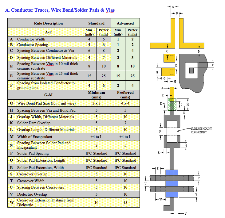
All applications supported by Silitronics requires to understand cutting edge design rules and state-of-the-art processing technology. Flip Chip BGA and wire bond BGA substrates are semiconductor packages with high reliability requiring line/space of 15/15 (12/12 R&D), Fine pitch laser vias, blind and buried vias, surface finish (ENIG, ENEPIG, SOP, SAC 305) options with Halogen-free and Lead-free BOM.


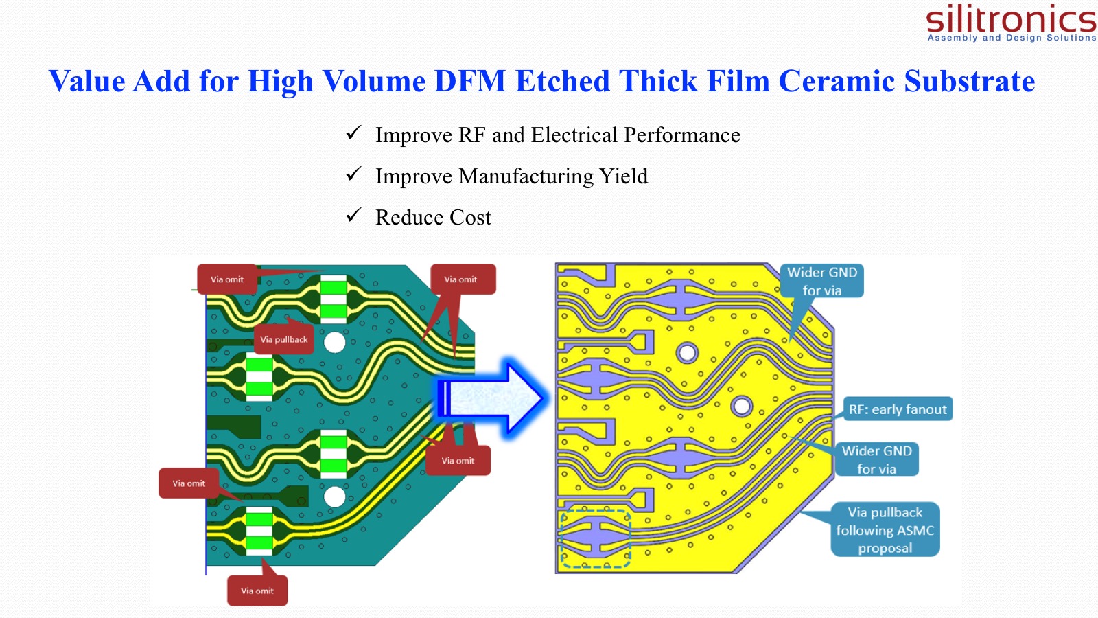
Ceramic Substrate (Etch Thick Film, HTCC, LTCC)
We follow customer’s design, electrical and mechanical requirement of the product. In order to help with time to market, our team understand end application and special design requirements; such as, component size, placement, interference, impedance, circuit routing, thermal constraints, environmental constraints, etc. Silitronics has the knowledge, experience and resources to handle complicated design requirements in order to provide the best possible product.
We are supplying high reliability substrates to the silicon photonics, LiDAR, aerospace, wireless, defense, industrial and medical applications. We can design the substrate by following customer’s net-list and schematic.


Advanced Assembly
(Gold Stud Bumping,Low Loop, Controlled Length,
Ribbon, Fine Pitch)
Silitronics team has over 100+ years of hands-on process development experience. With “Just Do It” attitude, in-house tooling design & fabrication, alongwith fully in-house automated equipment, allows Silitronics team to work with customers to “Push the Limit” with “Made In USA”. That helps customer with faster time to market and IP Protection.


Need more information on our Design Rules, Get in touch.
Your One-Stop Partner for
Advanced Semiconductor IC Packaging
Advanced Semiconductor IC Packaging