Why choose Silitronics?

20,000+ sq.ft.
State-of-the-Art
Facility:
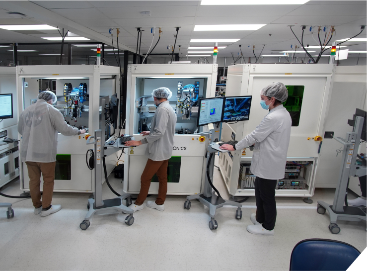
Equipped with 10K clean rooms and fully automated assembly lines for unparalleled precision.

One-Stop Solutions
From concept to finished product, we handle it all—design, assembly, testing, and delivery.

Cutting-Edge Equipment
From ±0.5μm flip chip placement to automatic wire bonding at 20μm pitch, we deliver unmatched accuracy.

Industry-Leading Speed
8-hour turnaround for urgent prototypes and 3-day cycle times for standard builds.

Proven
Expertise
99% yield on SiP modules and 90%+ yield on RF and flex assemblies.
Why choose Silitronics?

20,000+ sq.ft.
State-of-the-Art Facility:
Equipped with 10K clean rooms and fully automated assembly lines for unparalleled precision.

One-Stop Solutions
From concept to finished product, we handle it all—design, assembly, testing, and delivery.

Cutting-Edge Equipment
From ±0.5μm flip chip placement to automatic wire bonding at 20μm pitch, we deliver unmatched accuracy.

Industry-Leading Speed
8-hour turnaround for urgent prototypes and 3-day cycle times for standard builds.

Proven Expertise
99% yield on SiP modules and 90%+ yield on RF and flex assemblies.
We don’t just build semiconductor products, we engineer possibilities.
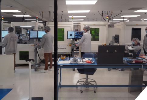
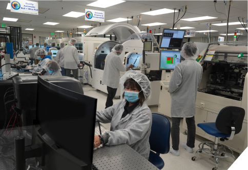
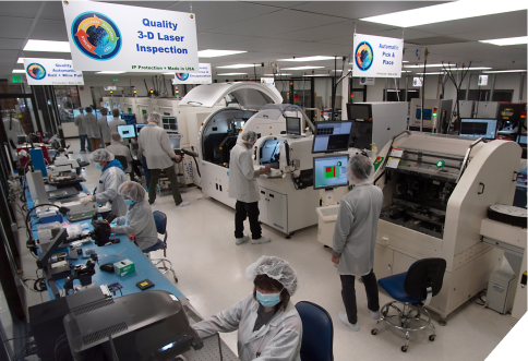
Located in the heart of Silicon Valley, our state-of-the-art facility is designed to deliver precision, reliability, and scalability for the most demanding industries.
With over 200+ years of collective expertise, we specialize in advanced semiconductor layout and assembly services, guided by our “First Time Right” philosophy. From prototyping to high-volume production, we ensure every product meets and exceeds your expectations.
We don't just build semiconductor products, we engineer possibilities.
Located in the heart of Silicon Valley, our state-of-the-art facility is designed to deliver precision, reliability, and scalability for the most demanding industries.
With over 200+ years of collective expertise, we specialize in advanced semiconductor layout and assembly services, guided by our "First Time Right" philosophy. From prototyping to high-volume production, we ensure every product meets and exceeds your expectations.
Built for Precision Manufacturing and Assembly. Designed for Breakthroughs.
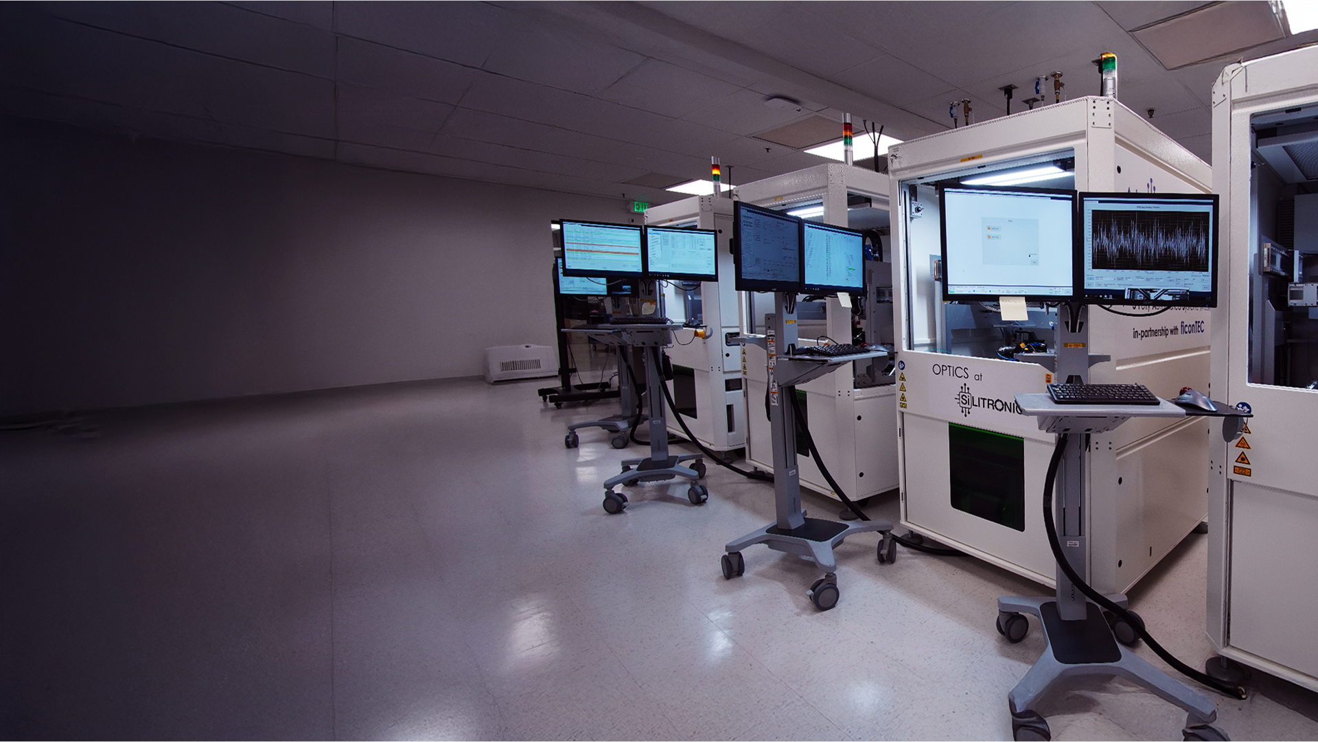
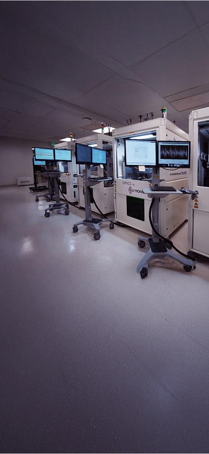
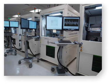
Our 1K and 10k clean rooms are the foundation of our commitment to quality. Designed to minimize contamination and cost, they ensure every product meets the highest standards of precision, performance and reliability.
Scalable. Reliable. Precision-Built.
Our System-in-Package (SiP) assembly capabilities are designed to meet the needs of the most advanced applications ranging from Defense to LiDAR, AR/VR, IoT and AI/ML. Our advanced engineering solutions ensure your products are built to outperform.
48,000/year
SiP Modules (PCBA + Wire Bonding + Glob Top + Testing) – 99% yield
60,000/year
RF Modules (Fine Pitch Wire Bonding + Low Loop) – 90% yield
60,000/year
Flex PCBA (Defense, Flexible Assemblies) – 90% yield
12,000/year
SiP (Optics Assembly + Wire Bonding + Testing) – 99% yield

Cutting-Edge Tools for
Cutting-Edge Solutions
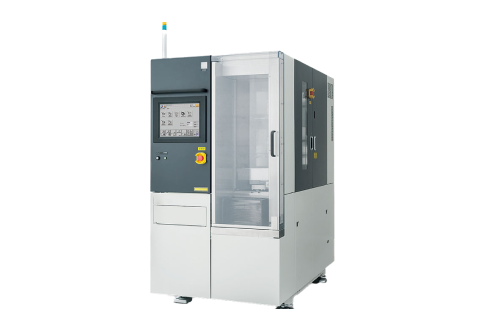
Our facility is equipped with the latest in semiconductor and photonics packaging technology. With in-house machine shops and weekend support for new NPI builds, we’re always ready to meet your deadlines.
Hermetic Sealing +
Eutectic Reflow
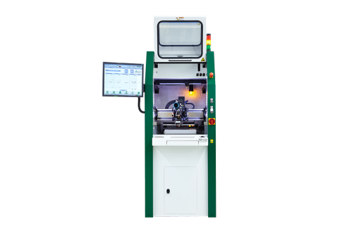
Auto Wedge Wire
Bonder
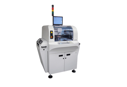
Auto Epoxy
Dispenser

See Precision in Action
Automatic Bonding for AR/VR:
60μm pitch, 140 wires - delivering unmatched accuracy for next-gen displays.
Active alignment for Silicon Photonics:
FAU Active Alignment for Silicon Photonics Enabling High Speed Data Transfer.
Auto Ball Bonding for IoT Sensors:
75μm loop height - ensuring reliability for smart, connected devices.
Get in touch
Interested in our end-to-end advanced semiconductor and photonics (PIC) packaging solutions?
Share your details for an expert connect.