
Chiplets services overview

Chiplet Co-Design
& Simulation
Full system design, partitioning, and simulation for complex architectures; modeling for scalability and reliability.

Heterogeneous
Assembly & Integration
Advanced assembly of diverse dies using state-of-the-art packaging and material science.

Interposer &
Stack Design
Silicon/organic interposers engineered for signal performance and scalable heterogeneous integration.

Screening &
Reliability
Validation
Rigorous electrical, thermal, screening & reliability validation.
Chiplets services overview
Chiplet Co-Design & Simulation
Full system design, partitioning, and simulation for complex architectures; modeling for scalability and reliability.
Heterogeneous Assembly & Integration
Advanced assembly of diverse dies using state-of-the-art packaging and material science.
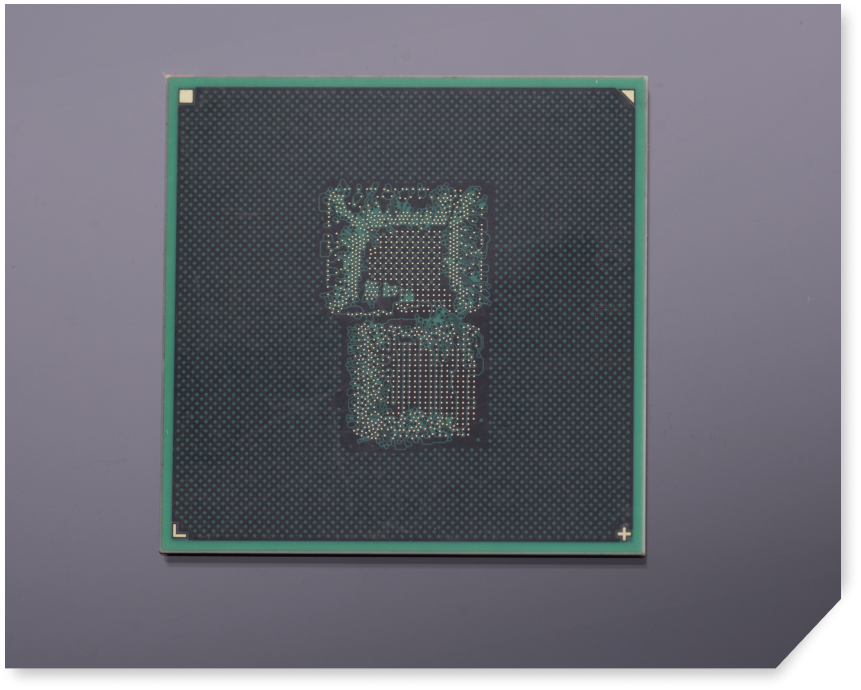
Interposer & Stack Design
Silicon/organic interposers engineered for signal performance and scalable heterogeneous integration.
Screening
& Reliability Validation
Rigorous electrical, thermal, screening & reliability validation.

Unlocking Tomorrow: Seamless Chiplet
Integration for Complex Systems


Chiplets Process Overview

Chiplet Partitioning & System-Level Design
Advanced algorithms guide function- and domain-based partitioning, optimizing wirelength, thermal coupling, and manufacturability. Silitronics consults closely with clients to model and simulate every aspect for fail-safe, scalable solutions.

Floorplan Optimization & Stack Co-Design
Proprietary simulation platforms analyze chiplet placement, bump mapping, and stack topology, balancing performance yield, SI/PI, and thermal spreading. Silitronics’ expertise ensures seamless stacking within interposer limits and package constraints.

Heterogeneous Assembly & Validation
Combines CPUs, memory, photonic and RF chiplets using advanced Fanout, TSV, and master bridges. Stress and thermal analysis are built into the process, with thorough pre/post integration testing guarantees every device’s field reliability.

Routing, Test, and Stress Screening
High-speed routing is simulated for electrical and thermal loads. All modules are subjected to burn-in, functional validation, and environmental stress before delivery—ensuring clients receive ready-to-deploy systems.
Chiplets Process Overview
Chiplet Partitioning & System-Level Design
Advanced algorithms guide function- and domain-based partitioning, optimizing wirelength, thermal coupling, and manufacturability. Silitronics consults closely with clients to model and simulate every aspect for fail-safe, scalable solutions.
Floorplan Optimization & Stack Co-Design
Proprietary simulation platforms analyze chiplet placement, bump mapping, and stack topology, balancing performance yield, SI/PI, and thermal spreading. Silitronics’ expertise ensures seamless stacking within interposer limits and package constraints.
Heterogeneous Assembly & Validation
Combines CPUs, memory, photonic and RF chiplets using advanced Fanout, TSV, and master bridges. Stress and thermal analysis are built into the process, with thorough pre/post integration testing guarantees every device’s field reliability.
Routing, Test, and Stress Screening
High-speed routing is simulated for electrical and thermal loads. All modules are subjected to burn-in, functional validation, and environmental stress before delivery—ensuring clients receive ready-to-deploy systems.
Chiplets Services Spectrum
Chiplet Co-Design
and Simulation
Silitronics provides end-to-end design, partitioning, and simulation for complex chiplet systems. Our team leverages electrical/thermal modeling to guarantee optimal, scalable architectures, from concept to production. .
Interposer and Stack
Design Services
Precision-crafted silicon or organic interposer designs, tailored for signal performance, thermal management, and scalable integration—key to next-generation systems.
Heterogeneous Assembly
& System Integration
Industry-leading assembly for digital, analog, photonic, and RF chiplets, tested for performance and environmental resilience, using advanced packaging and material science.

Screening, and
Reliability Validation
All chiplet modules undergo stringent electrical, thermal, and functional validation—ensuring best-in-class reliability and performance.
Chiplets Services Spectrum
Chiplet Co-Design
and Simulation
Silitronics provides end-to-end design, partitioning, and simulation for complex chiplet systems. Our team leverages electrical/thermal modeling to guarantee optimal, scalable architectures, from concept to production.
Interposer and Stack
Design Services
Precision-crafted silicon or organic interposer designs, tailored for signal performance, thermal management, and scalable integration—key to next-generation systems.
Heterogeneous Assembly
& System Integration
Industry-leading assembly for digital, analog, photonic, and RF chiplets, tested for performance and environmental resilience, using advanced packaging and material science.
Screening, and
Reliability Validation
All chiplet modules undergo stringent electrical, thermal, and functional validation—ensuring best-in-class reliability and performance.
Our Services Spectrum
Precision-Driven Design for
Next-Gen Semiconductor &
Photonic Packaging
From concept to layout, our advanced design expertise ensures seamless integration of chips, substrates, and interconnects. We optimize signal integrity, power efficiency, and thermal performance to meet the demands of AI accelerators, quantum computing, and high-speed photonic systems. With deep engineering insights, we design scalable, high-reliability solutions for the future.
LEARN MORE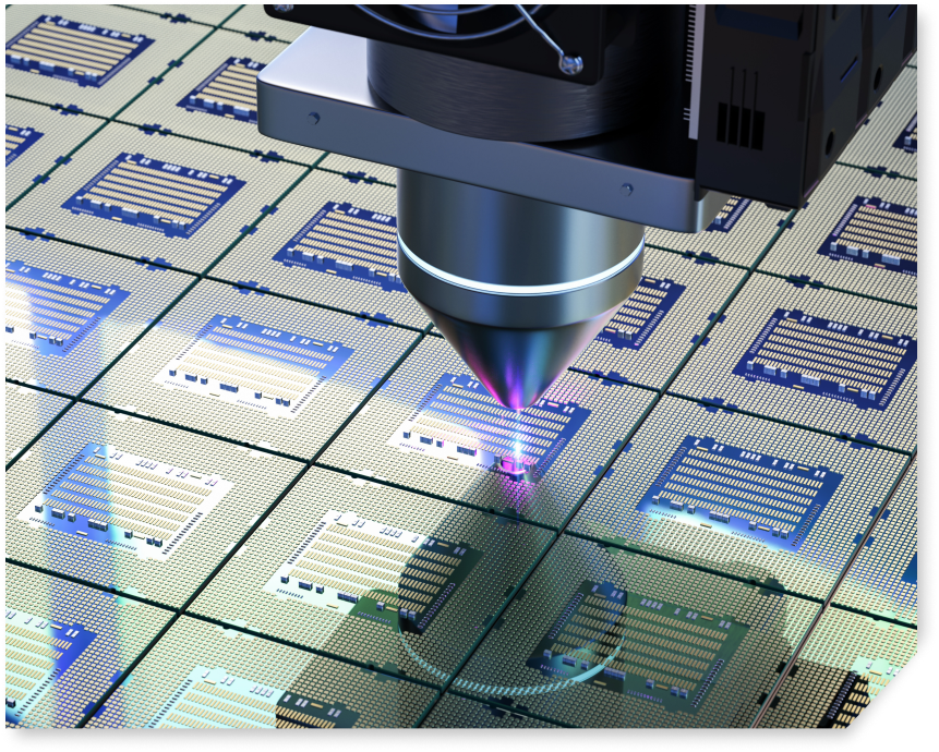
Fabrication for Advanced
Semiconductor & Photonic Packaging
Our state-of-the-art fabrication facility delivers high-precision multi-layer substrates tailored for AI, HPC, and Silicon Photonics. With expertise in organic and ceramic substrates, fine-pitch interconnects, and high-density integration, we ensure superior reliability, scalability, and manufacturing excellence. From prototypes to high-volume production, we bring innovation to life with precision.
LEARN MORE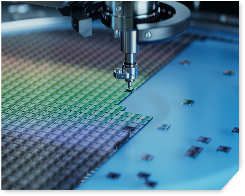
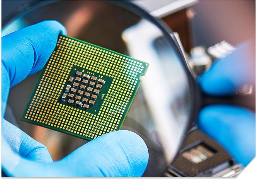
High-Precision Wafer Dicing
We deliver advanced wafer dicing using precision blade and laser technologies to ensure clean die separation with minimal chipping. Optimized for high yield and low particle contamination, our dicing supports next-gen semiconductor packaging and performance.
LEARN MORE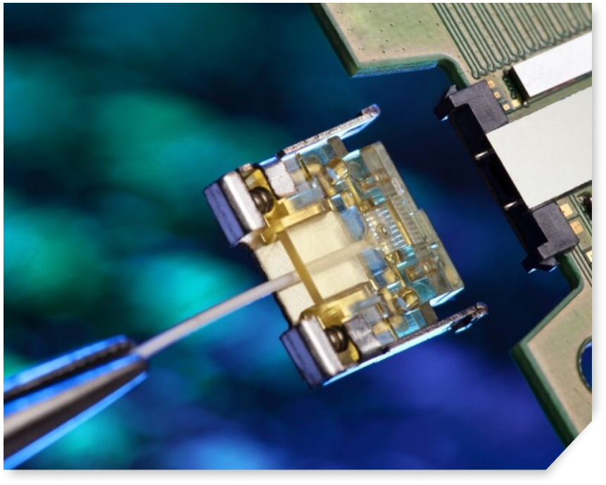
Powering the Future at the
Speed of Light with Photonics
Silicon Photonics is transforming high-speed computing, AI clusters, and next-gen data transfer. Our expertise in sub-micron active alignment, optical integration, and high-bandwidth packaging ensures low-latency, energy-efficient performance. From LiDAR to AI-driven interconnects, we deliver cutting-edge photonics solutions that push the limits of speed, scalability, and efficiency.
LEARN MORE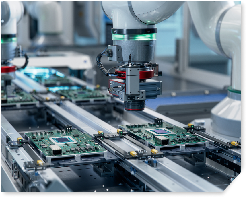
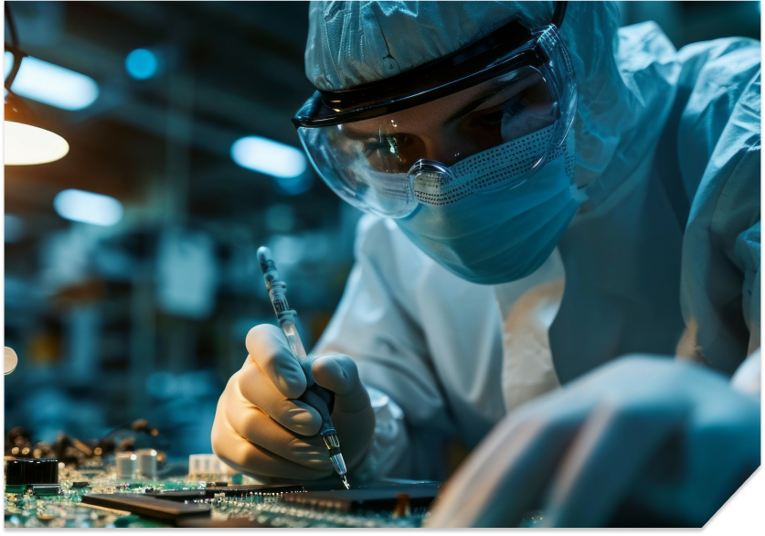
Seamless Assembly for High-Precision
Semiconductor & Photonic Packaging
Our cutting-edge assembly expertise ensures precise chip-to-package integration with industry-leading sub-micron active alignment, high-density interconnects, and heterogeneous integration. We specialize in complex optical and electronic assemblies for AI accelerators, 5G networks, and next-gen computing, delivering high-reliability solutions that optimize performance and reduce time to market.
LEARN MORE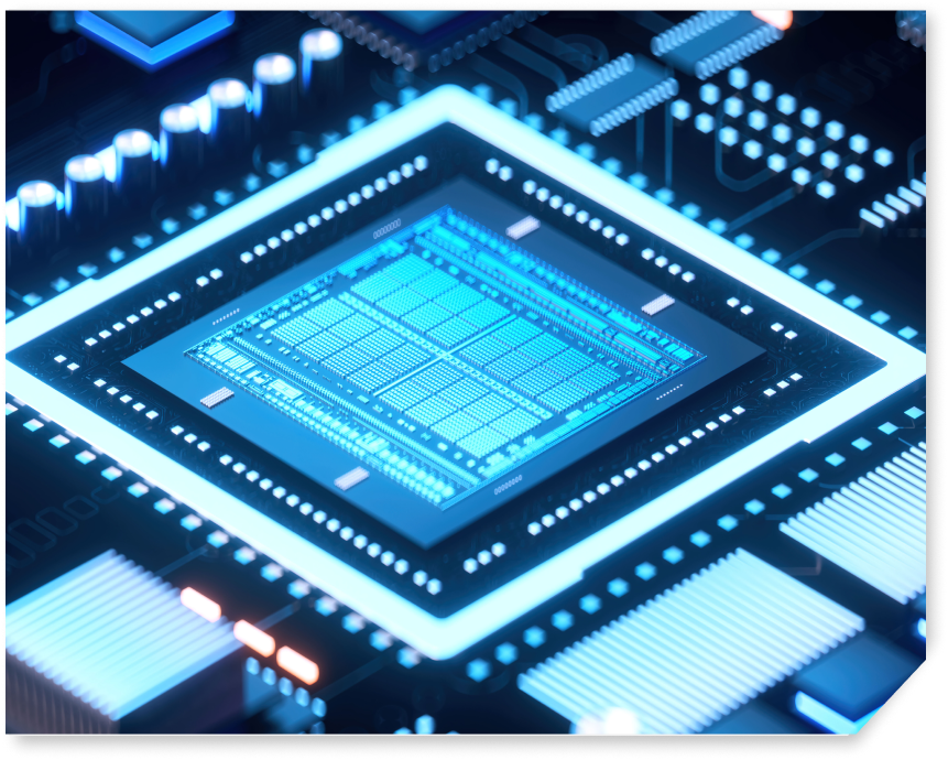
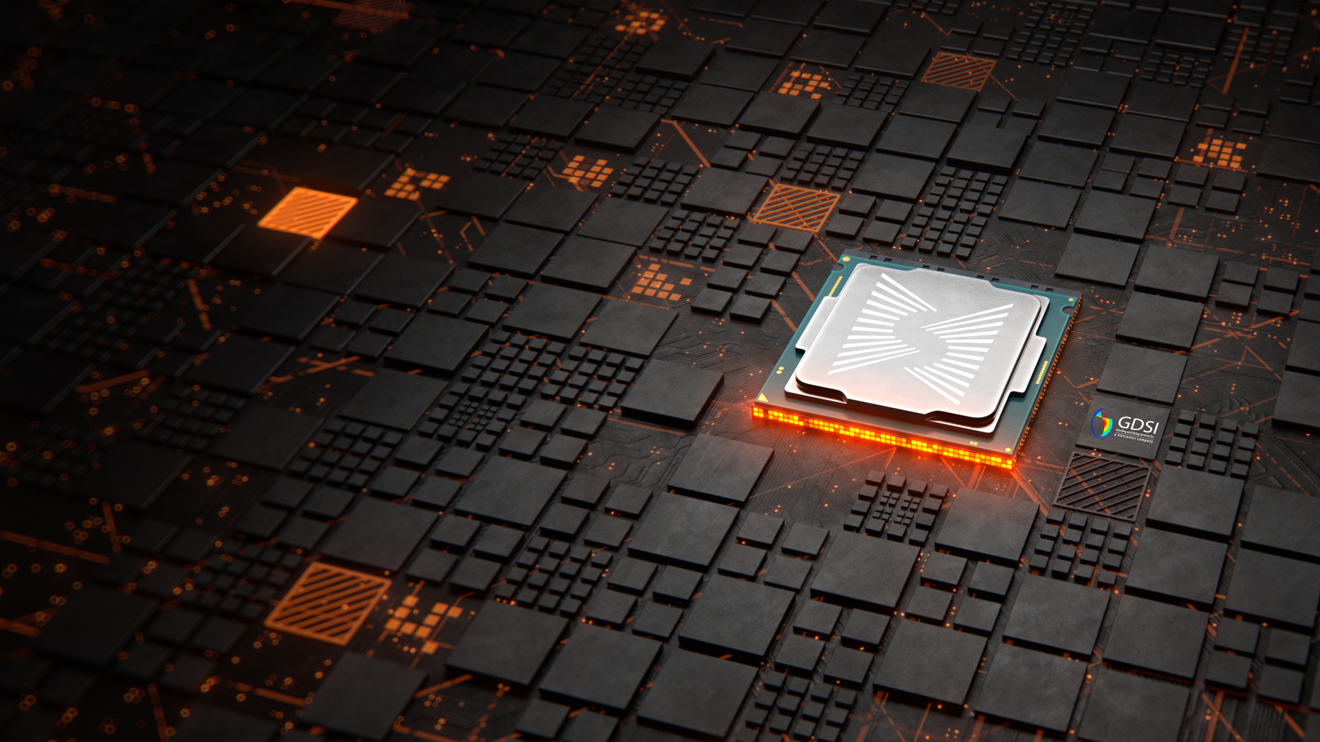
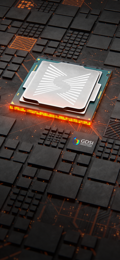
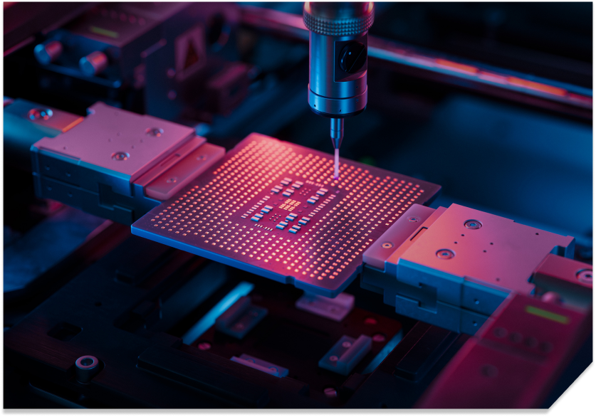
Breakthrough Chiplet Integration for
Scalable, Next-Gen Systems
Silitronics empowers the future of electronics with advanced chiplet integration—merging diverse dies on precision-engineered interposers for optimal signal, power, and thermal performance. Our expertise in modular floor planning and heterogeneous assembly accelerates high-bandwidth, low-latency connectivity that’s essential for AI, HPC, and 5G. From concept design to rigorous validation, Silitronics helps customers bring complex systems to market—faster, smarter, and more reliably.
LEARN MOREOur Services Spectrum
Precision-Driven Design for
Next-Gen Semiconductor
& Photonic
Packaging
From concept to layout, our advanced design expertise ensures seamless integration of chips, substrates, and interconnects. We optimize signal integrity, power efficiency, and thermal performance to meet the demands of AI accelerators, quantum computing, and high-speed photonic systems. With deep engineering insights, we design scalable, high-reliability solutions for the future.
LEARN MOREFabrication for AdvancedSemiconductor & Photonic Packaging
Our state-of-the-art fabrication facility delivers high-precision multi-layer substrates tailored for AI, HPC, and Silicon Photonics. With expertise in organic and ceramic substrates, fine-pitch interconnects, and high-density integration, we ensure superior reliability, scalability, and manufacturing excellence. From prototypes to high-volume production, we bring innovation to life with precision.
LEARN MOREHigh-Precision Wafer Dicing
We deliver advanced wafer dicing using precision blade and laser technologies to ensure clean die separation with minimal chipping. Optimized for high yield and low particle contamination, our dicing supports next-gen semiconductor packaging and performance.
LEARN MOREPowering the Future at the Speed of Light with Photonics
Silicon Photonics is transforming high-speed computing, AI clusters, and next-gen data transfer. Our expertise in sub-micron active alignment, optical integration, and high-bandwidth packaging ensures low-latency, energy-efficient performance. From LiDAR to AI-driven interconnects, we deliver cutting-edge photonics solutions that push the limits of speed, scalability, and efficiency.
LEARN MORESeamless Assembly for High-Precision Semiconductor & Photonic Packaging
Our cutting-edge assembly expertise ensures precise chip-to-package integration with industry-leading sub-micron active alignment, high-density interconnects, and heterogeneous integration. We specialize in complex optical and electronic assemblies for AI accelerators, 5G networks, and next-gen computing, delivering high-reliability solutions that optimize performance and reduce time to market.
LEARN MOREBreakthrough Chiplet Integration for Scalable, Next-Gen Systems
Silitronics empowers the future of electronics with advanced chiplet integration—merging diverse dies on precision-engineered interposers for optimal signal, power, and thermal performance. Our expertise in modular floor planning and heterogeneous assembly accelerates high-bandwidth, low-latency connectivity that’s essential for AI, HPC, and 5G. From concept design to rigorous validation, Silitronics helps customers bring complex systems to market—faster, smarter, and more reliably.
LEARN MORECase Studies
Accelerating Innovation in 4K Live Streaming & Gaming Cameras
Flawless execution, rapid prototyping, and first-pass success for cutting-edge automotive LiDAR technology.
Download case studyAccelerating Innovation in 4K Live Streaming & Gaming Cameras
First-pass success, rapid prototyping, and precision execution for breakthrough imaging technology.
Download case studyHigh-Yield, High-Precision IC Packaging for 5G & RF Innovation
Reliable, flexible, and high-performance IC packaging solutions, ensuring uninterrupted supply and exceptional quality.
Download case studyGet in touch
Interested in our end-to-end advanced semiconductor and photonics (PIC) packaging solutions?
Share your details for an expert connect.

Silitronics is your trusted one-stop partner for advanced semiconductor and photonics packaging–pushing the boundaries of design, fabrication, and assembly while driving sustainability.

Silitronics Solutions Inc 2388 Walsh Avenue, Santa Clara, CA, 95051
Email: sales@silitronics.com
Phone: +1 408-954-8301,
+1 408-605-1148


Grinding and Dicing Services Inc
925 Berryessa Road - San Jose, CA 95133
Email: sales@dieprepservices.com
Phone: +1 408 451 2000
+1 408 451 2000
© 2025 Silitronics. All rights reserved.
Silitronics is your trusted one-stop partner for advanced semiconductor and photonics packaging–pushing the boundaries of design, fabrication, and assembly while driving sustainability.
Silitronics Solutions Inc 2388 Walsh Avenue, Santa Clara, CA, 95051
Email: sales@silitronics.com
Phone: +1 408-954-8301,
+1 408-605-1148
© 2025 Silitronics. All rights reserved.