


Engineered Excellence in
Semiconductor &
Photonics Package Design
Schematic and Layout
- Schematics from datasheets or custom drawings, using industry-standard tools.
- Substrate selection: build-up vs. HDI via feasibility studies.
- Design and layout checked for rules and manufacturability before fab.
Signal Integrity
- SI/PI analysis with 2.5D/3D solvers and SPICE modeling.
- Time/frequency studies for crosstalk, impedance, and eye diagrams.
- Meets JEDEC signal integrity standards.
Power Integrity
- PDN checked for IR drop, AC impedance, and noise.
- Simulates die, package, and PCB power impacts.
- Design rules ensure reliable boards and substrates.
Build Up Boards
- Supports fine line/space, laser vias, blind/buried vias.
- Multiple finishes: ENIG, ENEPIG; all lead-free options.
- Designed for high reliability in flip chip/wire bond BGA.
Ceramic Substrate
- Custom designs for electrical and mechanical requirements.
- Handles complex routing, thermal and placement constraints.
- High-reliability for photonics, LiDAR, aerospace, and medical.
Advanced Assembly
- 100+ years' process expertise.
- In-house tooling and automation for fast turnaround.
- “Made in USA” for speed and IP protection.
Engineered Excellence in Semiconductor & Photonics Package Design
Schematic and Layout
- Schematics from datasheets or custom drawings, using industry-standard tools.
- Substrate selection: build-up vs. HDI via feasibility studies.
- Design and layout checked for rules and manufacturability before fab.
Signal Integrity
- SI/PI analysis with 2.5D/3D solvers and SPICE modeling.
- Time/frequency studies for crosstalk, impedance, and eye diagrams.
- Meets JEDEC signal integrity standards.
Power Integrity
- PDN checked for IR drop, AC impedance, and noise.
- Simulates die, package, and PCB power impacts.
- Design rules ensure reliable boards and substrates.
Build Up Boards
- Supports fine line/space, laser vias, blind/buried vias.
- Multiple finishes: ENIG, ENEPIG; all lead-free options.
- Designed for high reliability in flip chip/wire bond BGA.
Ceramic Substrate
- Custom designs for electrical and mechanical requirements.
- Handles complex routing, thermal and placement constraints.
- High-reliability for photonics, LiDAR, aerospace, and medical.
Advanced Assembly
- 100+ years' process expertise.
- In-house tooling and automation for fast turnaround.
- “Made in USA” for speed and IP protection.

Innovative Package Design, Engineered for Excellence


SiP Design Process & Capabilities

Define Architecture
- Substrate Technology Identification
- Component & Material Selection
- Signal Breakout & Fanout Strategies
- Prelayout PDN Design
- Thermal / Mechanical Plan

Design Input Parameters
- IO planning based on chip, package and board co-design
- Netlist Creation with Schematics / RTL / CSV etc
- Design rules & constraint setup
- IO + Placement Optimization

Package Layout
- Physical design using Cadence SiP, APD and Allegro
- Layer stack-up definition
- Component & IO Placement, Routing
- DFM & DFA Design Rules

Design Verification
- SI : Eye width/height, BER, Return loss, crosstalk
- PI : Target Z, IR drop, Ripple Noise analysis
- Thermal : Hot spots, Die temperature
- Mechanical: Warpage, Stress
- HFSS, Power SI, ADS
- DRC
- BOM Availability

Release To Manufacturing
- Design for Assembly (DFA)
- Design for Manufacturing (DFM)
- Reliability and Cost
SiP Design Capability
Define Architecture
- Substrate Technology Identification
- Component & Material Selection
- Signal Breakout & Fanout Strategies
- Prelayout PDN Design
- Thermal / Mechanical Plan
Define Architecture
- IO planning based on chip, package and board co-design
- Netlist Creation with Schematics / RTL / CSV etc
- Design rules & constraint setup
- IO + Placement Optimization
Define Architecture
- Physical design using Cadence SiP, APD and Allegro
- Layer stack-up definition
- Component & IO Placement, Routing
- DFM & DFA Design Rules
Define Architecture
- SI : Eye width/height, BER, Return loss, crosstalk
- PI : Target Z, IR drop, Ripple Noise analysis
- Thermal : Hot spots, Die temperature
- Mechanical: Warpage, Stress
- HFSS, Power SI, ADS
- DRC
- BOM Availability
Define Architecture
- Design for Assembly (DFA)
- Design for Manufacturing (DFM)
- Reliability and Cost
Design Services Spectrum
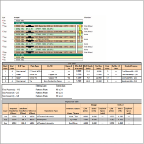
Schematic and Layout
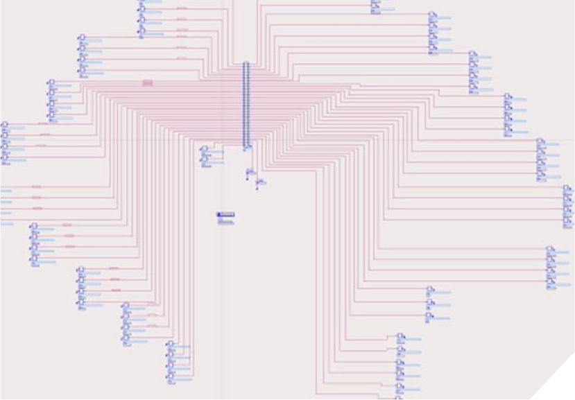
Using industry standard tools, Silitronics engineering team can create schematics from data sheets of merchant semiconductors or any custom drawing. We can do feasibility studies to select the best option between build up substrate or high density interconnect (HDI). After initial layout and SI/PI analysis, the design is reviewed to ensure design rules as well as DFM and DFA requirements are met before committing to FAB.
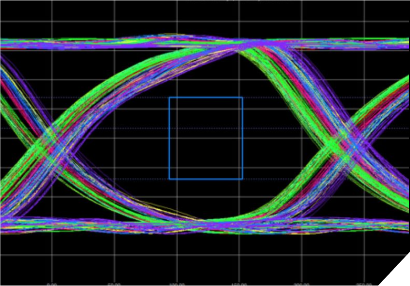
Signal Integrity
For applications requiring signal integrity (SI) and power integrity (PI) analysis, we work with the customer to understand their performance requirements. We use industry standard 2.5D and 3D field solvers to extract S-parameter model of the channel. Then, we fit the s-parameter model to a broadband spice model. Using this broadband SPICE channel model along with IBIS / IBIS-AMI models of the driver / receiver, we perform time / frequency domain analysis to study SI impairments such as crosstalk, impedance mismatch, and Eye diagrams. As an example, the figure on the right shows a simulated eye diagram of a LPDDR4X link connected to an ultra fine pitch SOC implemented on a SiP module with multilayer HDI stackup. As can be seen, the eye height and eye width meets the JEDEC mask specifications.
Power Integrity
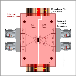
To validate power integrity, we check PDN (Power distribution Network) DC IR drop, AC impedance and ripple noise. As an example, figure on the left shows a detailed multiport model of a SERDES PDN which includes die, package and PCB models. Simulated PDN impedance and time domain ripple noise is also shown for reference
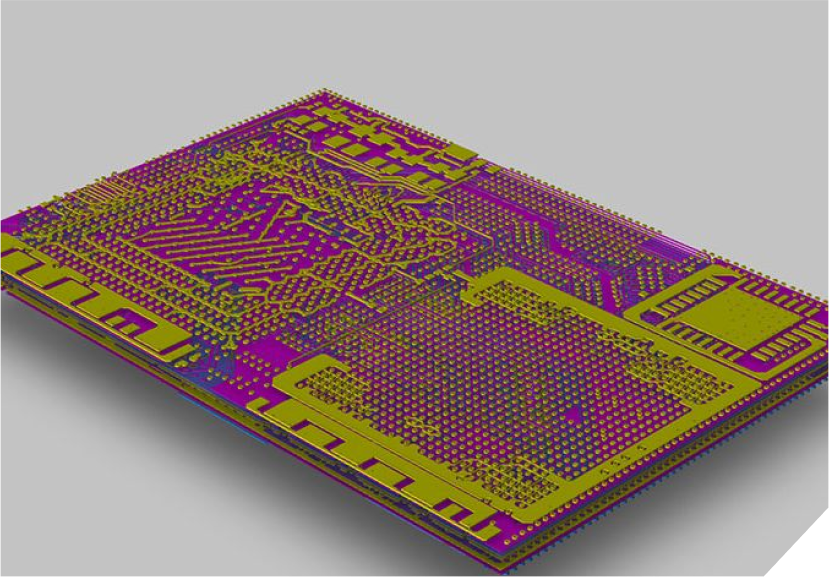
Build Up Boards
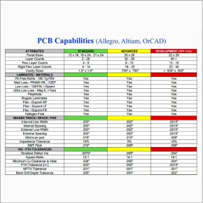
All applications supported by Silitronics requires to understand cutting edge design rules and state-of-the-art processing technology. Flip Chip BGA and wire bond BGA substrates are semiconductor packages with high reliability requiring line/space of 15/15 (12/12 R&D), Fine pitch laser vias, blind and buried vias, surface finish (ENIG, ENEPIG, SOP, SAC 305) options with Halogen-free and Lead-free BOM.
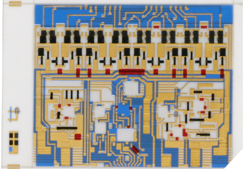
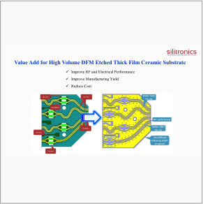
Ceramic Substrate
We follow customer’s design, electrical and mechanical requirement of the product. In order to help with time to market, our team understand end application and special design requirements; such as, component size, placement, interference, impedance, circuit routing, thermal constraints, environmental constraints, etc. Silitronics has the knowledge, experience and resources to handle complicated design requirements in order to provide the best possible product. We are supplying high reliability substrates to the silicon photonics, LiDAR, aerospace, wireless, defense, industrial and medical applications. We can design the substrate by following customer’s net-list and schematic.
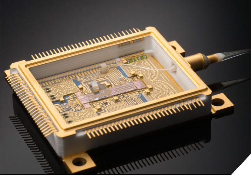
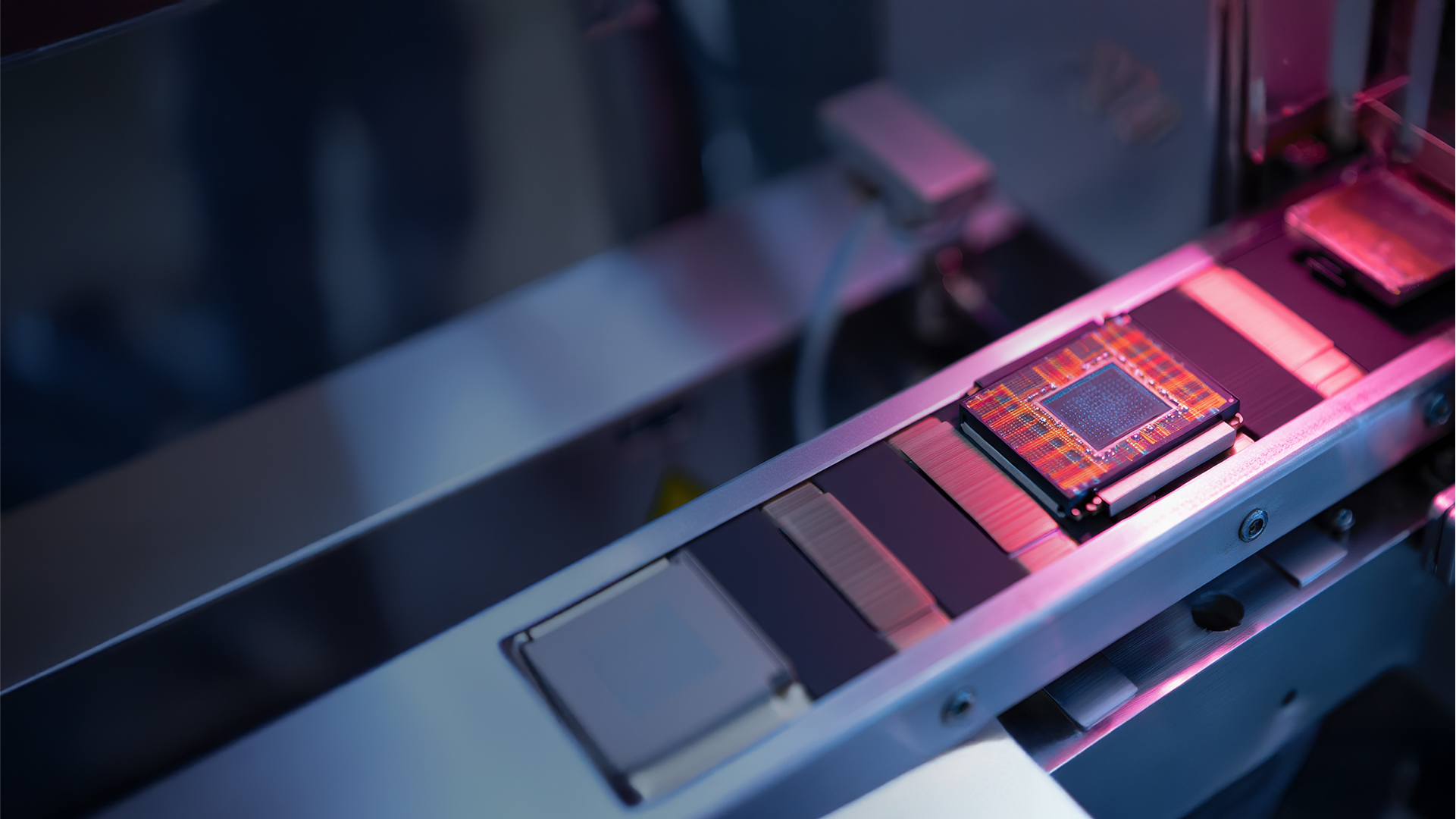
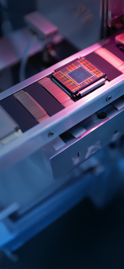
Advanced Assembly
Silitronics team has over 100+ years of hands-on process development experience. With “Just Do It” attitude, in-house tooling design & fabrication, alongwith fully in-house automated equipment, allows Silitronics team to work with customers to “Push the Limit” with “Made In USA”. That helps customer with faster time to market and IP Protection.
Design Rule
Design Rule
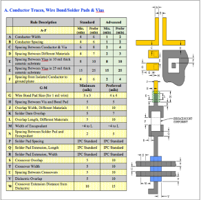
Silitronics has extensive Design Rules to guide customers when designing a new board, substrate or developing assembly processes.
Our Services Spectrum
Precision-Driven Design forNext-Gen Semiconductor & Photonic Packaging
From concept to layout, our advanced design expertise ensures seamless integration of chips, substrates, and interconnects. We optimize signal integrity, power efficiency, and thermal performance to meet the demands of AI accelerators, quantum computing, and high-speed photonic systems. With deep engineering insights, we design scalable, high-reliability solutions for the future.
LEARN MORE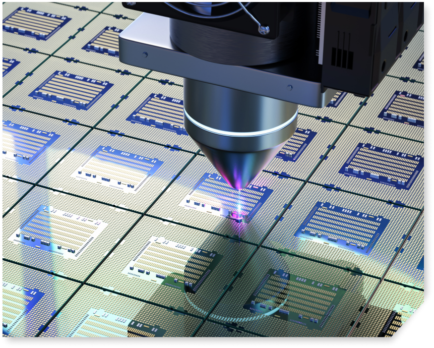
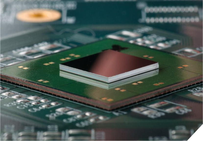
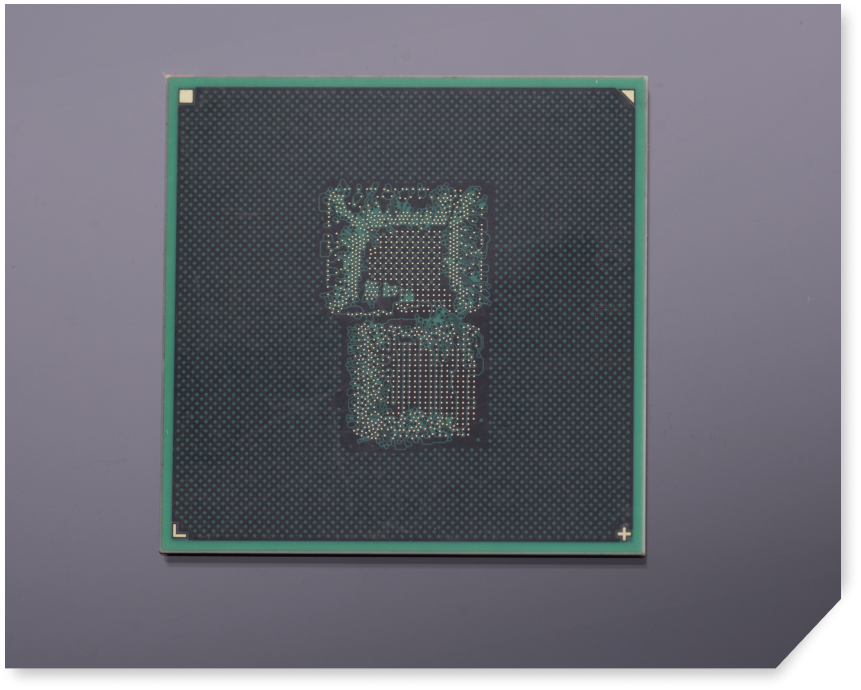
Fabrication for AdvancedSemiconductor & Photonic Packaging
Our state-of-the-art fabrication facility delivers high-precision multi-layer substrates tailored for AI, HPC, and Silicon Photonics. With expertise in organic and ceramic substrates, fine-pitch interconnects, and high-density integration, we ensure superior reliability, scalability, and manufacturing excellence. From prototypes to high-volume production, we bring innovation to life with precision.
LEARN MORE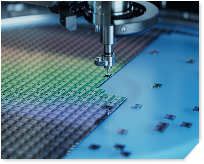
High-Precision Wafer Dicing
We deliver advanced wafer dicing using precision blade and laser technologies to ensure clean die separation with minimal chipping. Optimized for high yield and low particle contamination, our dicing supports next-gen semiconductor packaging and performance.
LEARN MORE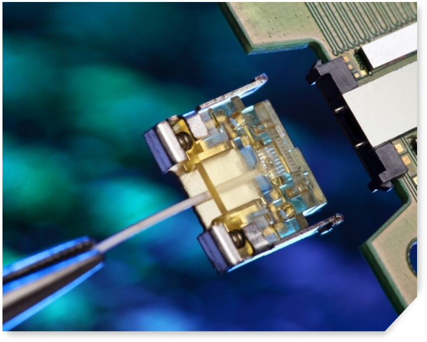
Powering the Future at the Speed of Light with Photonics
Silicon Photonics is transforming high-speed computing, AI clusters, and next-gen data transfer. Our expertise in sub-micron active alignment, optical integration, and high-bandwidth packaging ensures low-latency, energy-efficient performance. From LiDAR to AI-driven interconnects, we deliver cutting-edge photonics solutions that push the limits of speed, scalability, and efficiency.
LEARN MORE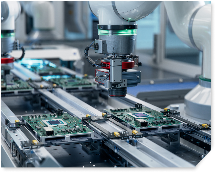
Seamless Assembly for High-Precision Semiconductor & Photonic Packaging
Our cutting-edge assembly expertise ensures precise chip-to-package integration with industry-leading sub-micron active alignment, high-density interconnects, and heterogeneous integration. We specialize in complex optical and electronic assemblies for AI accelerators, 5G networks, and next-gen computing, delivering high-reliability solutions that optimize performance and reduce time to market.
LEARN MORE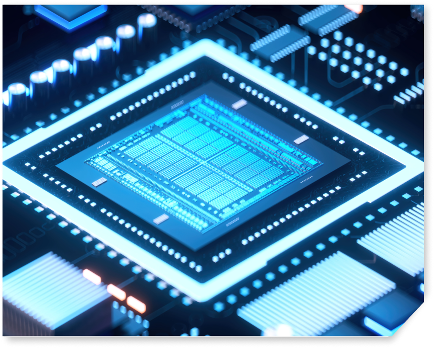
Breakthrough Chiplet Integration for Scalable, Next-Gen Systems
Silitronics empowers the future of electronics with advanced chiplet integration—merging diverse dies on precision-engineered interposers for optimal signal, power, and thermal performance. Our expertise in modular floor planning and heterogeneous assembly accelerates high-bandwidth, low-latency connectivity that’s essential for AI, HPC, and 5G. From concept design to rigorous validation, Silitronics helps customers bring complex systems to market—faster, smarter, and more reliably.
LEARN MOREOur Services Spectrum
Precision-Driven Design for
Next-Gen Semiconductor
& Photonic Packaging
From concept to layout, our advanced design expertise ensures seamless integration of chips, substrates, and interconnects. We optimize signal integrity, power efficiency, and thermal performance to meet the demands of AI accelerators, quantum computing, and high-speed photonic systems. With deep engineering insights, we design scalable, high-reliability solutions for the future.
LEARN MOREFabrication for AdvancedSemiconductor & Photonic Packaging
Our state-of-the-art fabrication facility delivers high-precision multi-layer substrates tailored for AI, HPC, and Silicon Photonics. With expertise in organic and ceramic substrates, fine-pitch interconnects, and high-density integration, we ensure superior reliability, scalability, and manufacturing excellence. From prototypes to high-volume production, we bring innovation to life with precision.
LEARN MOREHigh-Precision Wafer Dicing
We deliver advanced wafer dicing using precision blade and laser technologies to ensure clean die separation with minimal chipping. Optimized for high yield and low particle contamination, our dicing supports next-gen semiconductor packaging and performance.
LEARN MOREPowering the Future at the Speed of Light with Photonics
Silicon Photonics is transforming high-speed computing, AI clusters, and next-gen data transfer. Our expertise in sub-micron active alignment, optical integration, and high-bandwidth packaging ensures low-latency, energy-efficient performance. From LiDAR to AI-driven interconnects, we deliver cutting-edge photonics solutions that push the limits of speed, scalability, and efficiency.
LEARN MORESeamless Assembly for High-Precision Semiconductor & Photonic Packaging
Our cutting-edge assembly expertise ensures precise chip-to-package integration with industry-leading sub-micron active alignment, high-density interconnects, and heterogeneous integration. We specialize in complex optical and electronic assemblies for AI accelerators, 5G networks, and next-gen computing, delivering high-reliability solutions that optimize performance and reduce time to market.
LEARN MOREBreakthrough Chiplet Integration for Scalable, Next-Gen Systems
Silitronics empowers the future of electronics with advanced chiplet integration—merging diverse dies on precision-engineered interposers for optimal signal, power, and thermal performance. Our expertise in modular floor planning and heterogeneous assembly accelerates high-bandwidth, low-latency connectivity that’s essential for AI, HPC, and 5G. From concept design to rigorous validation, Silitronics helps customers bring complex systems to market—faster, smarter, and more reliably.
LEARN MORECase Studies
Driving Innovation in LiDAR with High-Precision SiP Packaging
Flawless execution, rapid prototyping, and first-pass success for cutting-edge automotive LiDAR technology.
Download case studyAccelerating Innovation in 4K Live Streaming & Gaming Cameras
First-pass success, rapid prototyping, and precision execution for breakthrough imaging technology.
Download case studyHigh-Yield, High-Precision IC Packaging for 5G & RF Innovation
Reliable, flexible, and high-performance IC packaging solutions, ensuring uninterrupted supply and exceptional quality.
Download case studyGet in touch
Interested in our end-to-end advanced semiconductor and photonics (PIC) packaging solutions?
Share your details for an expert connect.