


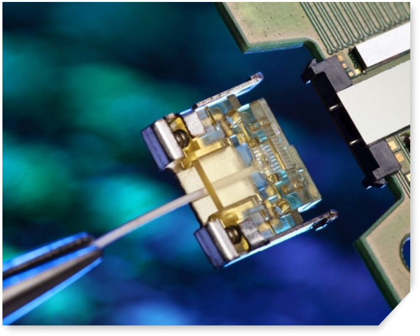
Silicon Photonics Services

Complete Photonics
Packaging & Assembly
End-to-end SOI device handling, FAU alignment, wire bonding, and encapsulation— ready for volume or prototype.

FAU & PIC Module
Integration
Multi-array fiber and photonic PIC alignment with real-time feedback; scalable modules for dense connectivity.

Optical Characterization
& Test Services
Beam profile, wavelength, loss, and system qualification in accordance with industry standards.

Co-Packaged Optics
Advanced 2.5D/3D integration for electronic-optic packaging in data center, sensing, and LiDAR applications.
Silicon Photonics Services
Complete Photonics Packaging & Assembly
End-to-end SOI device handling, FAU alignment, wire bonding, and encapsulation— ready for volume or prototype.
FAU & PIC Module Integration
Multi-array fiber and photonic PIC alignment with real-time feedback; scalable modules for dense connectivity.
Optical Characterization & Test Services
Beam profile, wavelength, loss, and system qualification in accordance with industry standards.
Co-Packaged Optics
Advanced 2.5D/3D integration for electronic-optic packaging in data center, sensing, lidar and quantum computing applications.

Redefining Optical Performance
with Silicon Photonics Expertise


Silicon Photonics Process Overview

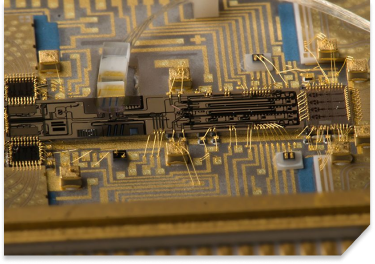
SOI Wafer Manufacturing & PIC Formation
Silitronics employs proprietary CMOS-compatible processes to fabricate waveguides, modulators, and detectors on SOI wafers. Careful control of etching, doping, and metallization ensures top bandwidth, low propagation loss, and optimal device uniformity—all benchmarked for telecom and datacom industry standards.

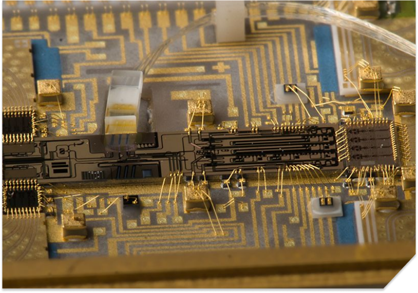
AU (Fiber Array Unit) Active Alignment
Automated active alignment rigs, with multi-axis feedback, achieve submicron fiber placement precision—up to ±0.5µm—into FAUs. Sophisticated process monitoring ensures minimal insertion loss and ultra-reliable coupling for 1x24 arrays and multi-channel photonics modules.

Edge Coupling and Mode Profile Testing
In-house test stations execute beam characterization, including mode field diameter, coupling efficiency, and polarization. Silitronics tailors coupling methods—edge, butt, or grating coupling—to meet device specs, ensuring stable performance across thermal and environmental shifts.

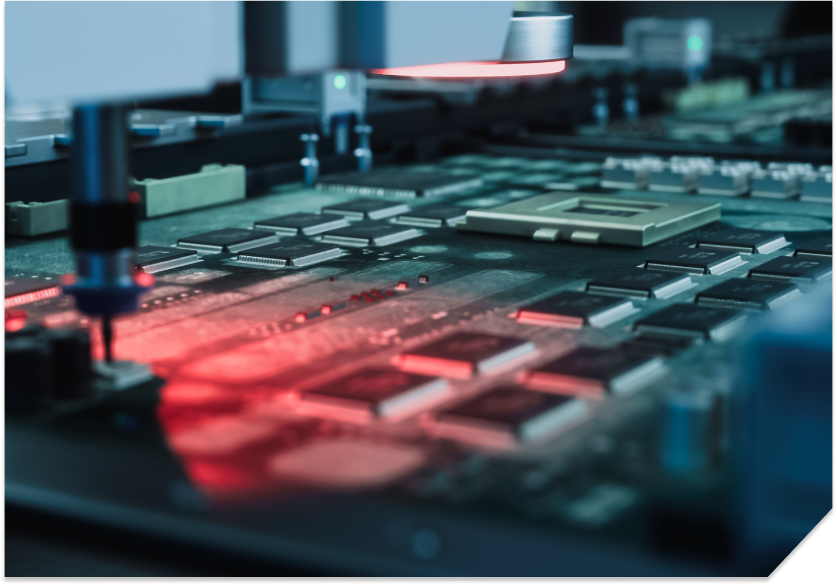
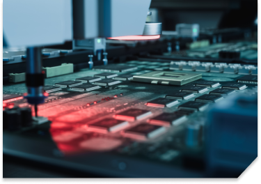
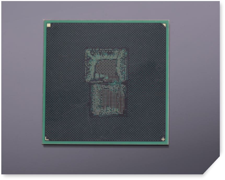
Co-Packaged Photonics Assembly & Reliability Screening
Leading in 2.5D and 3D integration, Silitronics co-packages electronic and optical chips, using cutting-edge die attach and encapsulation for superior throughput. Every module undergoes electrical and optical stress screening (eye diagram, BER, temperature cycling), setting industry benchmarks for reliability.
Silicon Photonics Process Overview
SOI Wafer Manufacturing & PIC Formation
Silitronics employs proprietary CMOS-compatible processes to fabricate waveguides, modulators, and detectors on SOI wafers. Careful control of etching, doping, and metallization ensures top bandwidth, low propagation loss, and optimal device uniformity—all benchmarked for telecom and datacom industry standards.
FAU (Fiber Array Unit) Active Alignment
Automated active alignment rigs, with multi-axis feedback, achieve submicron fiber placement precision—up to ±0.5µm—into FAUs. Sophisticated process monitoring ensures minimal insertion loss and ultra-reliable coupling for 1x24 arrays and multi-channel photonics modules.
Edge Coupling and Mode Profile Testing
In-house test stations execute beam characterization, including mode field diameter, coupling efficiency, and polarization. Silitronics tailors coupling methods—edge, butt, or grating coupling—to meet device specs, ensuring stable performance across thermal and environmental shifts.
Co-Packaged Photonics Assembly & Reliability Screening
Leading in 2.5D and 3D integration, Silitronics co-packages electronic and optical chips, using cutting-edge die attach and encapsulation for superior throughput. Every module undergoes electrical and optical stress screening (eye diagram, BER, temperature cycling), setting industry benchmarks for reliability.
Silicon Photonics Services Spectrum
Complete Photonics
Packaging & Assembly
SOI device handling, FAU design/build, active alignment, coupled with advanced wire bonding and module encapsulation—delivered turnkey for volume and prototyping.
Optical Characterization
& Test Services
Beam profile, wavelength tuning, loss metrics, and system qualification performed in-house. Full compliance with telecom/datacom standards (JEDEC, Telcordia, IEC).
FAU & PIC Module
Integration
Multi-channel FAU design for large-scale bandwidth with real-time optical feedback and loss calibration ensures ultra-efficient coupling and modular scalability.
Co-Packaged Optics for
Data Center & LiDAR
2.5D/3D integrated optical/electronic PIC solutions for hyperscale platforms, with full reliability screening and client-specific customization.
Silicon Photonics
Powering the Future at the Speed of Light with Photonics
Silicon Photonics is transforming high-speed computing, AI clusters, and next-gen data transfer. Our expertise in sub-micron active alignment, optical integration, and high-bandwidth packaging ensures low-latency, energy-efficient performance. From LiDAR to AI-driven interconnects, we deliver cutting-edge photonics solutions that push the limits of speed, scalability, and efficiency.
Silicon Photonics Services Spectrum
Complete Photonics Packaging & Assembly
SOI device handling, FAU design/build, active alignment, coupled with advanced wire bonding and module encapsulation—delivered turnkey for volume and prototyping.
Optical Characterization & Test Services
Beam profile, wavelength tuning, loss metrics, and system qualification performed in-house. Full compliance with telecom/datacom standards (JEDEC, Telcordia, IEC).
FAU & PIC Module Integration
Multi-channel FAU design for large-scale bandwidth with real-time optical feedback and loss calibration ensures ultra-efficient coupling and modular scalability.
Assembly
Co-Packaged Optics for Data Center & LiDAR
2.5D/3D integrated optical/electronic PIC solutions for hyperscale platforms, with full reliability screening and client-specific customization.
Our Services Spectrum
Precision-Driven Design for
Next-Gen Semiconductor &
Photonic Packaging
From concept to layout, our advanced design expertise ensures seamless integration of chips, substrates, and interconnects. We optimize signal integrity, power efficiency, and thermal performance to meet the demands of AI accelerators, quantum computing, and high-speed photonic systems. With deep engineering insights, we design scalable, high-reliability solutions for the future.
LEARN MORE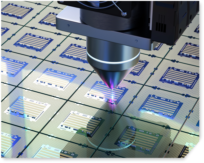
Fabrication for Advanced
Semiconductor & Photonic Packaging
Our state-of-the-art fabrication facility delivers high-precision multi-layer substrates tailored for AI, HPC, and Silicon Photonics. With expertise in organic and ceramic substrates, fine-pitch interconnects, and high-density integration, we ensure superior reliability, scalability, and manufacturing excellence. From prototypes to high-volume production, we bring innovation to life with precision.
LEARN MORE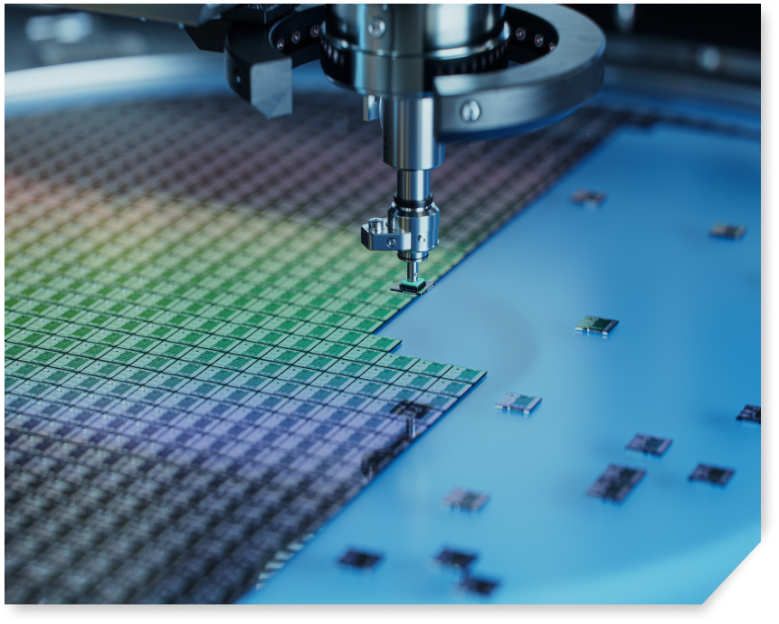
High-Precision Wafer Dicing
We deliver advanced wafer dicing using precision blade and laser technologies to ensure clean die separation with minimal chipping. Optimized for high yield and low particle contamination, our dicing supports next-gen semiconductor packaging and performance.
LEARN MORE
Powering the Future at the
Speed of Light with Photonics
Silicon Photonics is transforming high-speed computing, AI clusters, and next-gen data transfer. Our expertise in sub-micron active alignment, optical integration, and high-bandwidth packaging ensures low-latency, energy-efficient performance. From LiDAR to AI-driven interconnects, we deliver cutting-edge photonics solutions that push the limits of speed, scalability, and efficiency.
LEARN MORE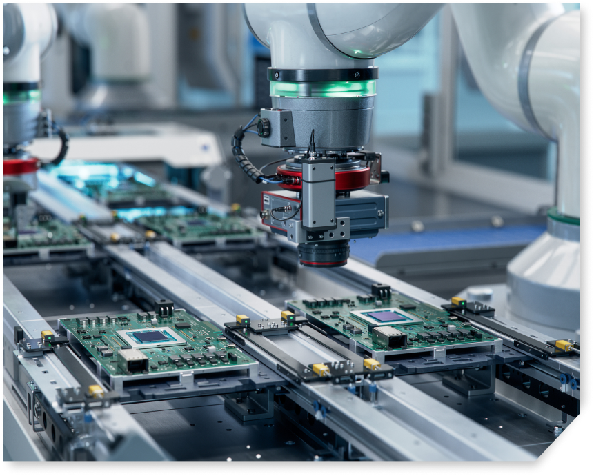
Seamless Assembly for High-Precision
Semiconductor & Photonic Packaging
Our cutting-edge assembly expertise ensures precise chip-to-package integration with industry-leading sub-micron active alignment, high-density interconnects, and heterogeneous integration. We specialize in complex optical and electronic assemblies for AI accelerators, 5G networks, and next-gen computing, delivering high-reliability solutions that optimize performance and reduce time to market.
LEARN MORE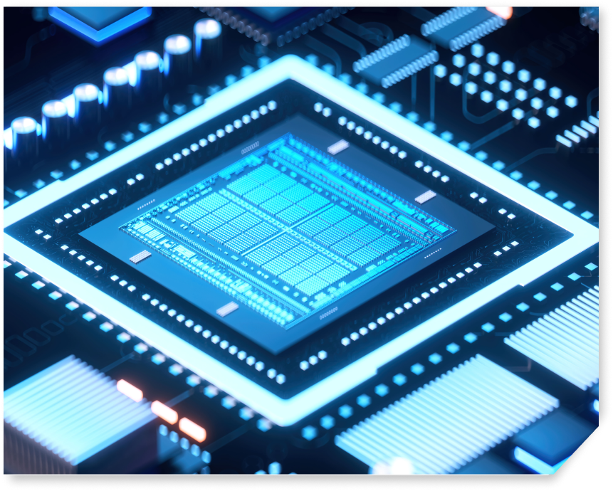
Breakthrough Chiplet Integration for
Scalable, Next-Gen Systems
Silitronics empowers the future of electronics with advanced chiplet integration—merging diverse dies on precision-engineered interposers for optimal signal, power, and thermal performance. Our expertise in modular floor planning and heterogeneous assembly accelerates high-bandwidth, low-latency connectivity that’s essential for AI, HPC, and 5G. From concept design to rigorous validation, Silitronics helps customers bring complex systems to market—faster, smarter, and more reliably.
LEARN MOREOur Services Spectrum
Precision-Driven Design for
Next-Gen Semiconductor
& Photonic
Packaging
From concept to layout, our advanced design expertise ensures seamless integration of chips, substrates, and interconnects. We optimize signal integrity, power efficiency, and thermal performance to meet the demands of AI accelerators, quantum computing, and high-speed photonic systems. With deep engineering insights, we design scalable, high-reliability solutions for the future.
LEARN MOREFabrication for AdvancedSemiconductor & Photonic Packaging
Our state-of-the-art fabrication facility delivers high-precision multi-layer substrates tailored for AI, HPC, and Silicon Photonics. With expertise in organic and ceramic substrates, fine-pitch interconnects, and high-density integration, we ensure superior reliability, scalability, and manufacturing excellence. From prototypes to high-volume production, we bring innovation to life with precision.
LEARN MOREHigh-Precision Wafer Dicing
We deliver advanced wafer dicing using precision blade and laser technologies to ensure clean die separation with minimal chipping. Optimized for high yield and low particle contamination, our dicing supports next-gen semiconductor packaging and performance.
LEARN MOREPowering the Future at the Speed of Light with Photonics
Silicon Photonics is transforming high-speed computing, AI clusters, and next-gen data transfer. Our expertise in sub-micron active alignment, optical integration, and high-bandwidth packaging ensures low-latency, energy-efficient performance. From LiDAR to AI-driven interconnects, we deliver cutting-edge photonics solutions that push the limits of speed, scalability, and efficiency.
LEARN MORESeamless Assembly for High-Precision Semiconductor & Photonic Packaging
Our cutting-edge assembly expertise ensures precise chip-to-package integration with industry-leading sub-micron active alignment, high-density interconnects, and heterogeneous integration. We specialize in complex optical and electronic assemblies for AI accelerators, 5G networks, and next-gen computing, delivering high-reliability solutions that optimize performance and reduce time to market.
LEARN MOREBreakthrough Chiplet Integration for Scalable, Next-Gen Systems
Silitronics empowers the future of electronics with advanced chiplet integration—merging diverse dies on precision-engineered interposers for optimal signal, power, and thermal performance. Our expertise in modular floor planning and heterogeneous assembly accelerates high-bandwidth, low-latency connectivity that’s essential for AI, HPC, and 5G. From concept design to rigorous validation, Silitronics helps customers bring complex systems to market—faster, smarter, and more reliably.
LEARN MORECase Studies
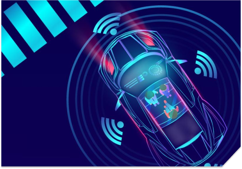
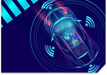
Flawless execution, rapid prototyping, and first-pass success for cutting-edge automotive LiDAR technology.
Flawless execution, rapid prototyping, and first-pass success for cutting-edge automotive LiDAR technology.
Download case studyAccelerating Innovation in 4K Live Streaming & Gaming Cameras
First-pass success, rapid prototyping, and precision execution for breakthrough imaging technology.
Download case studyHigh-Yield, High-Precision IC Packaging for 5G & RF Innovation
Reliable, flexible, and high-performance IC packaging solutions, ensuring uninterrupted supply and exceptional quality.
Download case studyGet in touch
Interested in our end-to-end advanced semiconductor and photonics (PIC) packaging solutions?
Share your details for an expert connect.