


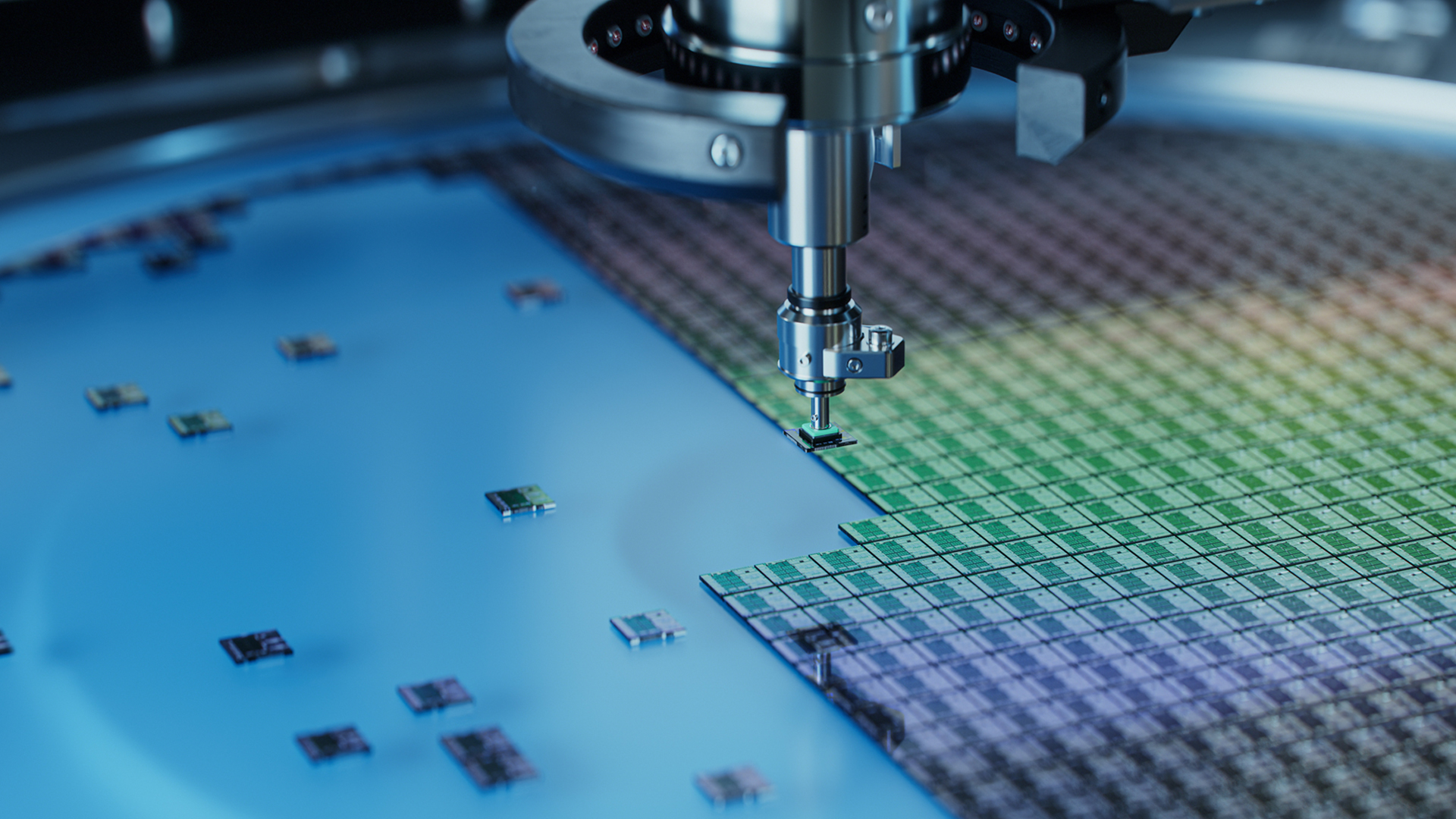
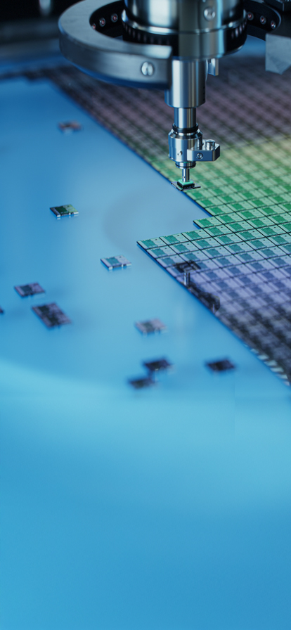
Dicing services overview
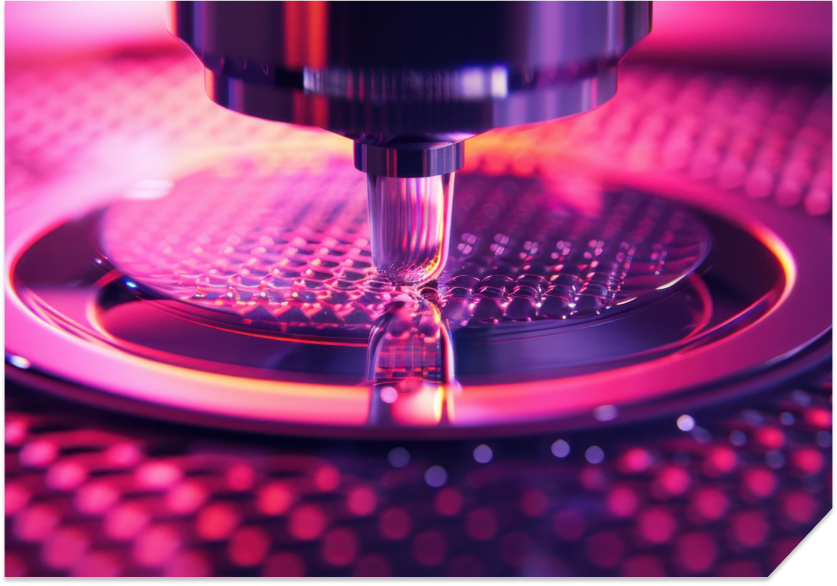
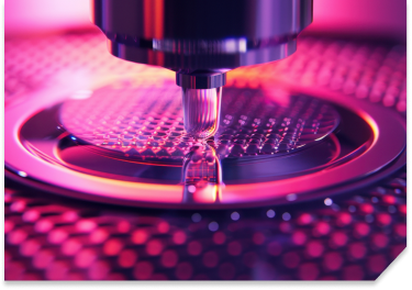
Stealth Laser
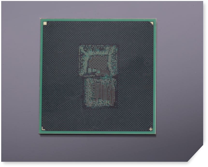
Dicing for PICs
Ultra-clean, non-contact singulation of photonic devices; minimal edge damage, optimal yield.

Wafer Thinning
& Polishing
Controlled thinning and CMP for smooth, reliable dies; supports silicon photonics and advanced packaging.

Standard Mechanical
Wafer Dicing
Diamond blade dicing for silicon, compound semiconductors, ceramics, and glass in volume or specialty runs.

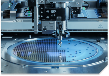
Automated AOI, Sorting,
Pick and Place
Automated Inspection, sorting, and safe pick and place for defect-free, ready-to-use dies.
Dicing services overview
Stealth Laser Dicing for PICs
Ultra-clean, non-contact singulation of photonic devices; minimal edge damage, optimal yield.
Wafer Thinning & Polishing
Controlled thinning and CMP for smooth, reliable dies; supports silicon photonics and advanced packaging.
Standard Mechanical
Wafer Dicing
Diamond blade dicing for silicon, compound semiconductors, ceramics, and glass in volume or specialty runs.
Automated AOI, Sorting,
Pick and Placeg
Headline: Automated AOI, Sorting, Pick and Place Sub-head: Automated Inspection, sorting, and safe pick and place for defect-free, ready-to-use dies. replace highlighted word with - silicon photonics

Unmatched Precision in Wafer
Dicing & Die Singulation


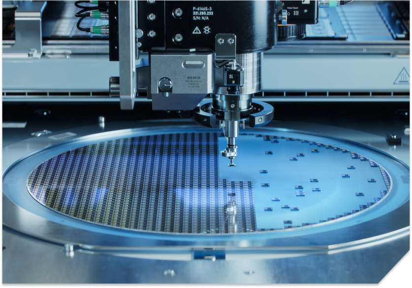
Dicing Process Overview

Wafer Preparation & Mounting
Every process starts with ultrasonic wafer cleaning, flatness measurement, and careful mounting on dicing tape. Silitronics ensures precise alignment and minimal contamination, using anti-static environments and calibrated carriers for maximum handling safety and first-pass accuracy.

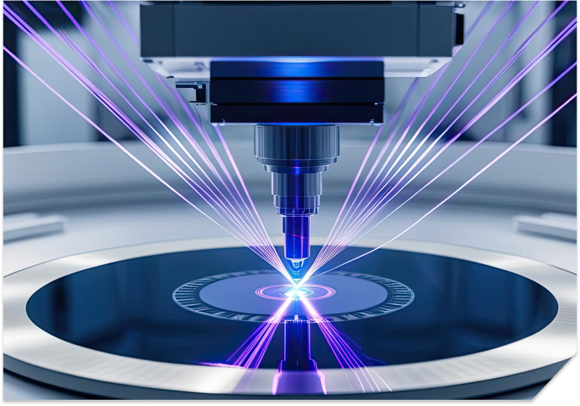
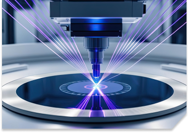
Dicing Techniques: Blade, Stealth Laser, Plasma
Silitronics tailors dicing techniques: diamond blade for standard dies, stealth laser for fragile PICs, and plasma for ultra-fine pitch. Each is optimized for kerf width, cut speed, and minimal thermal/mechanical stress. Engineers continuously monitor blade wear and laser calibration for consistent die quality, even in high-mix product runs.

Wafer Thinning & Polishing
Chemical and mechanical thinning down to sub-100µm is performed in humidity-controlled zones. Polished wafers—especially for photonics—receive additional CMP steps to achieve mirror surfaces, reducing insertion loss and supporting high-yield optical coupling.

Automated Optical Inspection (AOI) & Sorting
Post-dicing, every die undergoes AOI for cracks, chips, contamination,
and
dimensional accuracy. Defective dies are sorted out, while clean dies
are
ultrasonically cleaned, dried, and automatically sorted for
traceability
and
next-stage fabrication.

Final Cleaning & Packaging
Finished dies receive anti-static handling, laser marking, and custom tray or tape-and-reel packaging, all designed for shipment integrity and downstream assembly reliability.
Dicing
Process Overview
Wafer Preparation & Mounting
Every process starts with ultrasonic wafer cleaning, flatness measurement, and careful mounting on dicing tape. Silitronics ensures precise alignment and minimal contamination, using anti-static environments and calibrated carriers for maximum handling safety and first-pass accuracy.
Dicing Techniques:Blade, Stealth Laser, Plasma
Silitronics tailors dicing techniques: diamond blade for standard dies, stealth laser for fragile PICs, and plasma for ultra-fine pitch. Each is optimized for kerf width, cut speed, and minimal thermal/mechanical stress. Engineers continuously monitor blade wear and laser calibration for consistent die quality, even in high-mix product runs.
Wafer Thinning & Polishing
Chemical and mechanical thinning down to sub-100µm is performed in humidity-controlled zones. Polished wafers—especially for photonics—receive additional CMP steps to achieve mirror surfaces, reducing insertion loss and supporting high-yield optical coupling.
Automated Optical Inspection (AOI) & Sorting
Post-dicing, every die undergoes AOI for cracks, chips, contamination, and dimensional accuracy. Defective dies are sorted out, while clean dies are ultrasonically cleaned, dried, and automatically sorted for traceability and next-stage fabrication.
Final Cleaning & Packaging
Finished dies receive anti-static handling, laser marking, and custom tray or tape-and-reel packaging, all designed for shipment integrity and downstream assembly reliability.
Dicing Services Spectrum
Stealth Laser Dicing for Photonic
Integrated Circuits (PICs)
Stealth laser enables non-contact singulation
of PICs, minimizing
stress
and
edge
damage for
high-performance and ultra-sensitive devices.
Silitronics’
proprietary process delivers top
yield and edge cleanliness, critical
for
data
and optical communications.
Standard Wafer Dicing for
Semiconductor and
Compound
Materials
Diamond blade dicing suited for silicon, GaAs,
ceramic, and
glass
wafers, with proven
reliability and scalable throughput.
Customizable
blade
selection and process
parameters allow for tailored solutions for
unique
device
requirements.
Wafer Thinning and Polishing
Controlled thinning for high-speed logic,
photonics, and MEMS
platforms, enabling thinner
devices with improved thermal and
mechanical
performance. Post-thinning CMP ensures
consistently smooth surfaces,
optimized
for
assembly, optics, and device longevity.

Automated AOI, Sorting,
and Final Packaging
High-resolution inspection, binning, and safe
packaging
guarantee
each die is defect-free and
production-ready. Silitronics’ QC-driven
approach
provides clear traceability across
every wafer, batch, and customer
order.
Dicing Services
Spectrum
Stealth Laser Dicing for Photonic
Integrated Circuits (PICs)
Stealth laser enables non-contact
singulation of PICs,
minimizing
stress and
edge damage for high-performance and ultra-
sensitive
devices.
Silitronics’ proprietary
process delivers top yield and edge
cleanliness,
critical for data and optical
communications.
Standard Wafer Dicing for
Semiconductor and
Compound
Materials
Diamond blade dicing suited for silicon, GaAs,
ceramic, and
glass
wafers, with proven
reliability and scalable throughput.
Customizable
blade
selection and process
parameters allow for tailored solutions for
unique
device
requirements.
Wafer Thinning and Polishing
Controlled thinning for high-speed logic,
photonics, and
MEMS
platforms, enabling
thinner devices with improved thermal and
mechanical
performance. Post-thinning CMP
ensures consistently smooth surfaces,
optimized
for assembly, optics, and device
longevity.

Automated AOI, Sorting, and
Final Packaging
High-resolution inspection, binning,
and safe packaging
guarantee
each die is
defect-free and production-ready.
Silitronics’ QC-driven
approach
provides
clear traceability across every wafer,
batch, and customer
order.
Our Services Spectrum
Precision-Driven Design for
Next-Gen Semiconductor &
Photonic Packaging
From concept to layout, our advanced design expertise ensures seamless integration of chips, substrates, and interconnects. We optimize signal integrity, power efficiency, and thermal performance to meet the demands of AI accelerators, quantum computing, and high-speed photonic systems. With deep engineering insights, we design scalable, high-reliability solutions for the future.
LEARN MORE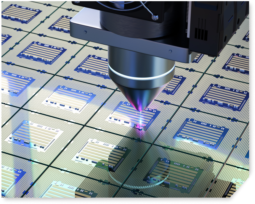
Fabrication for Advanced
Semiconductor & Photonic Packaging
Our state-of-the-art fabrication facility delivers high-precision multi-layer substrates tailored for AI, HPC, and Silicon Photonics. With expertise in organic and ceramic substrates, fine-pitch interconnects, and high-density integration, we ensure superior reliability, scalability, and manufacturing excellence. From prototypes to high-volume production, we bring innovation to life with precision.
LEARN MORE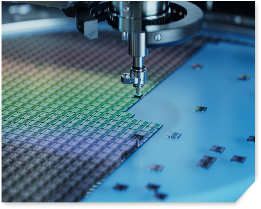
High-Precision Wafer Dicing
We deliver advanced wafer dicing using precision blade and laser technologies to ensure clean die separation with minimal chipping. Optimized for high yield and low particle contamination, our dicing supports next-gen semiconductor packaging and performance.
LEARN MORE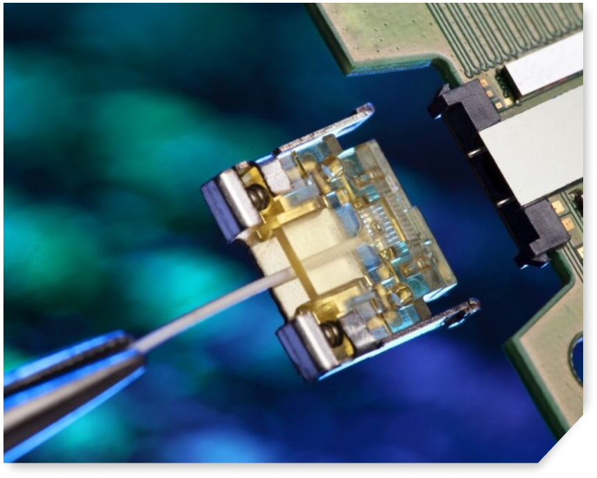
Powering the Future at the
Speed of Light with Photonics
Silicon Photonics is transforming high-speed computing, AI clusters, and next-gen data transfer. Our expertise in sub-micron active alignment, optical integration, and high-bandwidth packaging ensures low-latency, energy-efficient performance. From LiDAR to AI-driven interconnects, we deliver cutting-edge photonics solutions that push the limits of speed, scalability, and efficiency.
LEARN MORE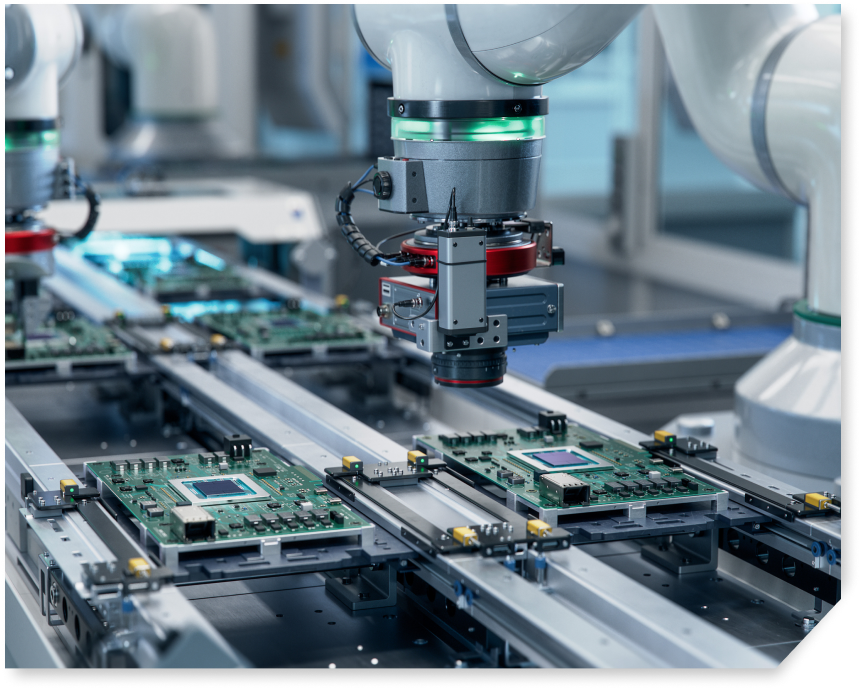
Seamless Assembly for High-Precision
Semiconductor & Photonic Packaging
Our cutting-edge assembly expertise ensures precise chip-to-package integration with industry-leading sub-micron active alignment, high-density interconnects, and heterogeneous integration. We specialize in complex optical and electronic assemblies for AI accelerators, 5G networks, and next-gen computing, delivering high-reliability solutions that optimize performance and reduce time to market.
LEARN MORE
Breakthrough Chiplet Integration for
Scalable, Next-Gen Systems
Silitronics empowers the future of electronics with advanced chiplet integration—merging diverse dies on precision-engineered interposers for optimal signal, power, and thermal performance. Our expertise in modular floor planning and heterogeneous assembly accelerates high-bandwidth, low-latency connectivity that’s essential for AI, HPC, and 5G. From concept design to rigorous validation, Silitronics helps customers bring complex systems to market—faster, smarter, and more reliably.
LEARN MOREOur Services Spectrum
Precision-Driven Design for
Next-Gen Semiconductor
& Photonic
Packaging
From concept to layout, our advanced design expertise ensures seamless integration of chips, substrates, and interconnects. We optimize signal integrity, power efficiency, and thermal performance to meet the demands of AI accelerators, quantum computing, and high-speed photonic systems. With deep engineering insights, we design scalable, high-reliability solutions for the future.
LEARN MOREFabrication for AdvancedSemiconductor & Photonic Packaging
Our state-of-the-art fabrication facility delivers high-precision multi-layer substrates tailored for AI, HPC, and Silicon Photonics. With expertise in organic and ceramic substrates, fine-pitch interconnects, and high-density integration, we ensure superior reliability, scalability, and manufacturing excellence. From prototypes to high-volume production, we bring innovation to life with precision.
LEARN MOREHigh-Precision Wafer Dicing
We deliver advanced wafer dicing using precision blade and laser technologies to ensure clean die separation with minimal chipping. Optimized for high yield and low particle contamination, our dicing supports next-gen semiconductor packaging and performance.
LEARN MOREPowering the Future at the Speed of Light with Photonics
Silicon Photonics is transforming high-speed computing, AI clusters, and next-gen data transfer. Our expertise in sub-micron active alignment, optical integration, and high-bandwidth packaging ensures low-latency, energy-efficient performance. From LiDAR to AI-driven interconnects, we deliver cutting-edge photonics solutions that push the limits of speed, scalability, and efficiency.
LEARN MORESeamless Assembly for High-Precision Semiconductor & Photonic Packaging
Our cutting-edge assembly expertise ensures precise chip-to-package integration with industry-leading sub-micron active alignment, high-density interconnects, and heterogeneous integration. We specialize in complex optical and electronic assemblies for AI accelerators, 5G networks, and next-gen computing, delivering high-reliability solutions that optimize performance and reduce time to market.
LEARN MOREBreakthrough Chiplet Integration for Scalable, Next-Gen Systems
Silitronics empowers the future of electronics with advanced chiplet integration—merging diverse dies on precision-engineered interposers for optimal signal, power, and thermal performance. Our expertise in modular floor planning and heterogeneous assembly accelerates high-bandwidth, low-latency connectivity that’s essential for AI, HPC, and 5G. From concept design to rigorous validation, Silitronics helps customers bring complex systems to market—faster, smarter, and more reliably.
LEARN MORECase Studies
Flawless execution, rapid prototyping, and first-pass success for cutting-edge automotive LiDAR technology.
First-pass success, rapid prototyping, and precision execution for breakthrough imaging technology.
Download case studyAccelerating Innovation in 4K Live Streaming & Gaming Cameras
First-pass success, rapid prototyping, and precision execution for breakthrough imaging technology.
Download case studyHigh-Yield, High-Precision IC Packaging for 5G & RF Innovation
Reliable, flexible, and high-performance IC packaging solutions, ensuring uninterrupted supply and exceptional quality.
Download case studyGet in touch
Interested in our end-to-end advanced semiconductor and photonics (PIC) packaging solutions?
Share your details for an expert connect.