


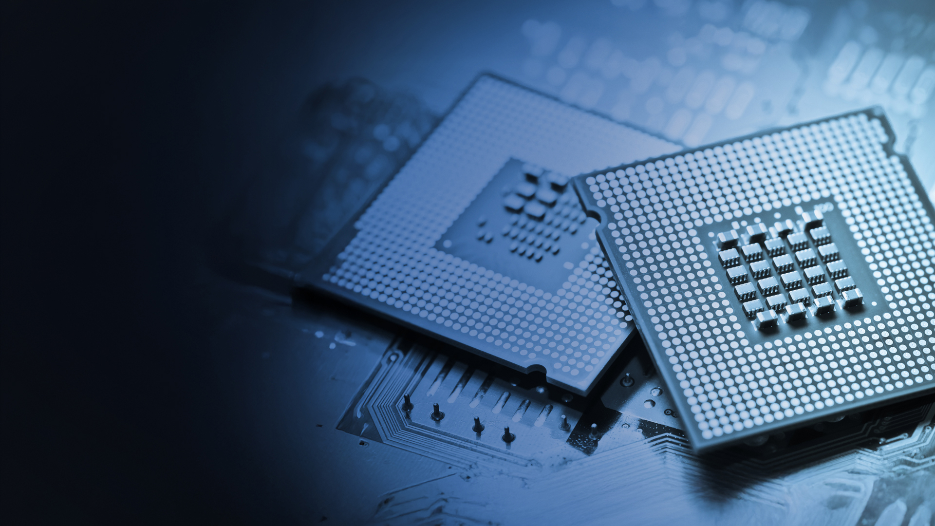

Fabrication services overview

Organic Build-Up
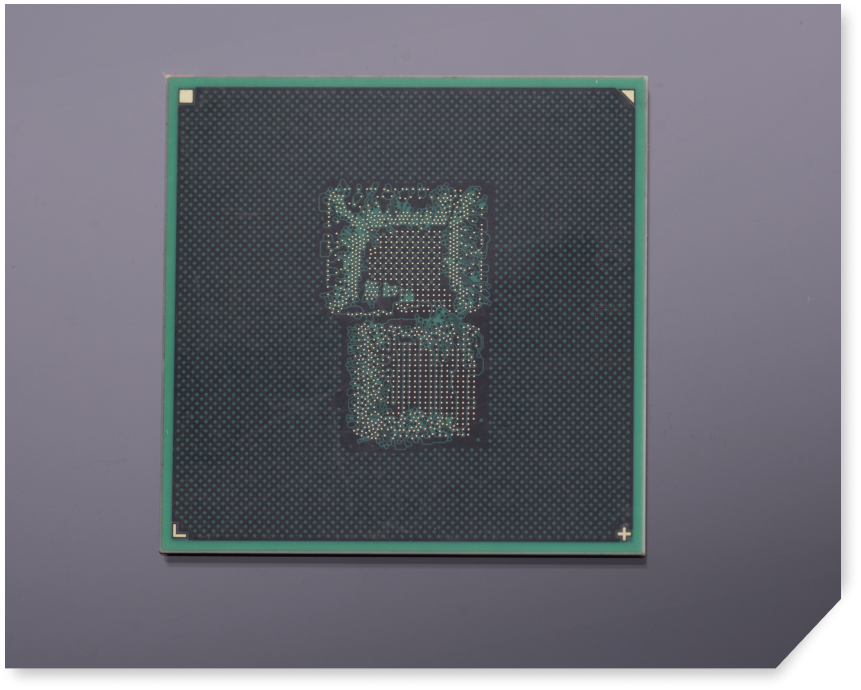
Substrates
High-speed multilayer build-up with fine
line/space, thin core, and embedded
passives
for custom applications.

HDI & Fine-Pitch
Substrate Design
State-of-the-art microvia and blind/buried via processing for next-gen integration, SiP,and photonics modules.

Ceramic Substrates
(HTCC/LTCC)
Precision ceramics with thick film metallization and advanced tape lamination for wireless, RF, and harsh environments.

Rapid Prototyping &
Volume Manufacturing
Agile sampling and scalable production—high yield from first prototype to full deployment.
Fabrication services overview
Organic Build-Up Substrates
High-speed multilayer build-up with fine line/space, thin core, and embedded passives for custom applications.
HDI & Fine-Pitch Substrate Design
State-of-the-art microvia and blind/buried via processing for next-gen integration, SiP, and photonics modules.
Ceramic Substrates (HTCC/LTCC)
Precision ceramics with thick film metallization and advanced tape lamination for wireless, RF, and harsh environments.
Rapid Prototyping & Volume Manufacturing
Agile sampling and scalable production—high yield from first prototype to full deployment.

Pioneering the Future of Advanced
Substrate Manufacturing


Fabrication Process Overview

Material Selection & Lamination
Each substrate starts with careful material selection—BT, ABF, or ceramic bases tailored for electrical, thermal, and mechanical needs. Sophisticated lamination controls produce uniform core thickness and optimal dielectric properties, forming the foundation for reliable, high-density interconnects in complex stack-ups.

Microvia Formation & Drilling
Utilizing both mechanical and precision laser drilling, Silitronics produces microvias at sub-15µm sizes for dense layouts. Advanced laser techniques allow formation of blind/buried vias in multilayer boards, critical for HDI and next-gen designs. Every drill cycle is monitored for registration and via integrity to prevent signal loss.

Circuit Patterning & Metallization
Dry film lamination and photolithography precisely create circuit features down to 10/10 µm. High-quality copper plating ensures controlled impedance and robust signal performance, while state-of-the-art etching selectively removes unwanted metal. The result is consistently accurate trace geometry in every substrate.

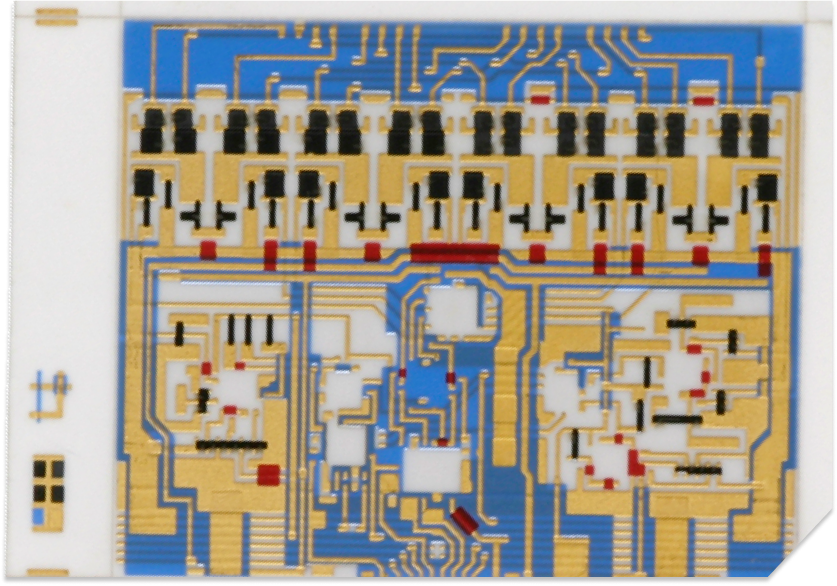
Ceramic Processing (HTCC/LTCC)
Silitronics engineers ceramic substrates using tape lamination, screen printing, and high-temperature sintering. These processes enable reliable thick film metallization and precise conductor patterns for harsh environment and RF applications. Meticulous polishing delivers perfect surface finishes vital for photonics and sensing platforms.

Surface Treatment & AOI
Substrates receive premium finishes including ENIG, ENEPIG and OSP, supporting solderability and corrosion resistance. Automated Optical Inspection (AOI) and electrical testing rigorously validate layer registration and circuit continuity, guaranteeing process reliability and readiness for advanced assembly.

Profiling, Cutting & Final QA
Each substrate is precisely profiled and cut to custom dimensions, undergoes final inspection, and receives full process documentation to aid traceability and support regulatory requirements. This end-to-end approach eliminates hidden defects and assures high-yield downstream integration.
Fabrication Process Overview
Material Selection & Lamination
Each substrate starts with careful material selection—BT, ABF, or ceramic bases tailored for electrical, thermal, and mechanical needs. Sophisticated lamination controls produce uniform core thickness and optimal dielectric properties, forming the foundation for reliable, high-density interconnects in complex stack-ups.
Microvia Formation & Drilling
Utilizing both mechanical and precision laser drilling, Silitronics produces microvias at sub-15µm sizes for dense layouts. Advanced laser techniques allow formation of blind/buried vias in multilayer boards, critical for HDI and next-gen designs. Every drill cycle is monitored for registration and via integrity to prevent signal loss.
Define Architecture
Dry film lamination and photolithography precisely create circuit features down to 10/10 µm. High-quality copper plating ensures controlled impedance and robust signal performance, while state-of-the-art etching selectively removes unwanted metal. The result is consistently accurate trace geometry in every substrate.
Surface Treatment & AOI
Substrates receive premium finishes including ENIG, ENEPIG and OSP, supporting solderability and corrosion resistance. Automated Optical Inspection (AOI) and electrical testing rigorously validate layer registration and circuit continuity, guaranteeing process reliability and readiness for advanced assembly.
Profiling, Cutting & Final QA
Each substrate is precisely profiled and cut to custom dimensions, undergoes final inspection, and receives full process documentation to aid traceability and support regulatory requirements. This end-to-end approach eliminates hidden defects and assures high-yield downstream integration.
Fabrication Services Spectrum

Organic Build-Up Substrates
High-speed multilayer build-up substrates with fine line/space, thin core, and embedded passives. Silitronics provides full customization for networking, AI, and medical platforms, ensuring superior signal integrity and thermal handling, from rapid prototyping to high-volume production.
Ceramic Substrates
(Etch Thick Film, HTCC, LTCC)
Specializing in robust ceramics for wireless, sensor, and RF applications. Employing advanced tape lamination and metallization processes, Silitronics delivers ceramics with precise conductor layouts, superior environmental resilience, and polished surfaces for optimum device performance.
HDI & Fine-Pitch Substrate Design
State-of-the-art microvia, blind/buried via, and tightly controlled copper thickness enable next-gen integration for silicon photonics, SiP, and multichip modules. Designed for high reliability, superior SI/PI, and production scalability.
Rapid Prototyping & Volume
Manufacturing
Silitronics offers agile prototyping—delivering functional substrates fast—alongside robust volume manufacturing, maintaining process repeatability, high yield, and rigorous documentation from the first sample to full-scale deployment.
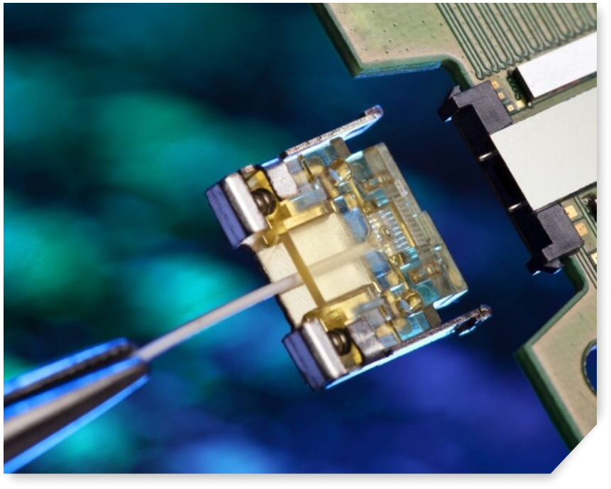
Silicon Photonics
Powering the Future at the Speed of Light with Photonics
Silicon Photonics is transforming high-speed computing, AI clusters, and next-gen data transfer. Our expertise in sub-micron active alignment, optical integration, and high-bandwidth packaging ensures low-latency, energy-efficient performance. From LiDAR to AI-driven interconnects, we deliver cutting-edge photonics solutions that push the limits of speed, scalability, and efficiency.
LEARN MOREFabrication Services Spectrum
Organic Build-Up Substrates
High-speed multilayer build-up substrates with fine line/space, thin core, and embedded passives. Silitronics provides full customization for networking, AI, and medical platforms, ensuring superior signal integrity and thermal handling, from rapid prototyping to high-volume production.
Ceramic Substrates (Etch Thick Film, HTCC, LTCC)
Our state-of-the-art fabrication facility delivers high-precision multi-layer substrates tailored for AI, HPC, and Silicon Photonics. With expertise in organic and ceramic substrates, fine-pitch interconnects, and high-density integration, we ensure superior reliability, scalability, and manufacturing excellence. From prototypes to high-volume production, we bring innovation to life with precision.
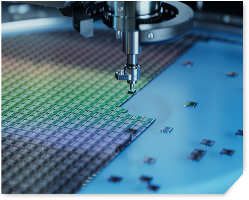
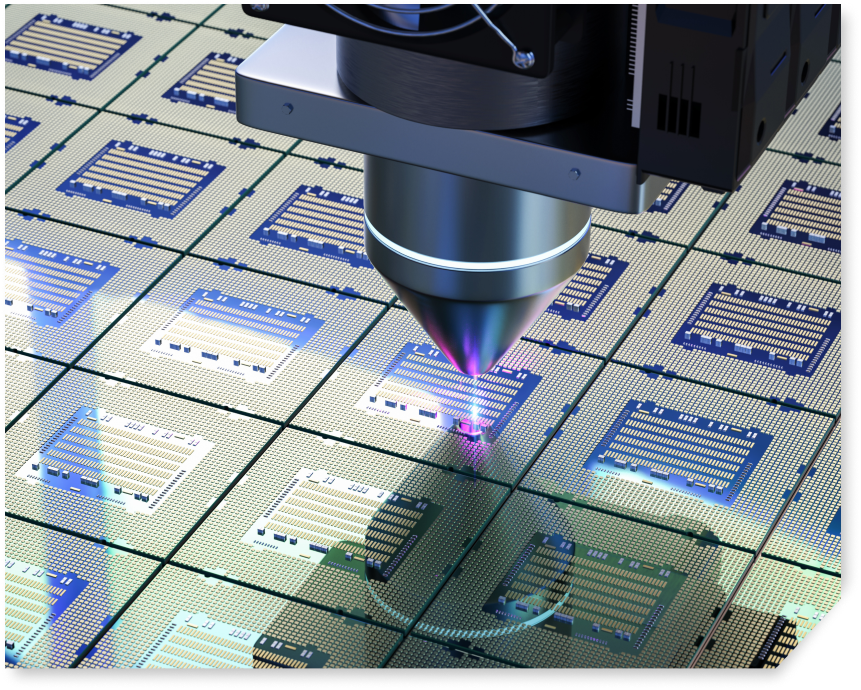
Dicing
High-Precision Wafer Dicing
Specializing in robust ceramics for wireless, sensor, and RF applications. Employing advanced tape lamination and metallization processes, Silitronics delivers ceramics with precise conductor layouts, superior environmental resilience, and polished surfaces for optimum device performance.
HDI & Fine-Pitch Substrate Design
State-of-the-art microvia, blind/buried via, and tightly controlled copper thickness enablenext-gen integration for silicon photonics, SiP, and multichip modules. Designed for high reliability, superior SI/PI, and production scalability.
Rapid Prototyping & Volume Manufacturing
Silitronics offers agile prototyping—delivering functional substrates fast—alongside robust volume manufacturing, maintaining process repeatability, high yield, and rigorous documentation from the first sample to full-scale deployment.
Our Services Spectrum
Precision-Driven Design for
Next-Gen Semiconductor &
Photonic Packaging
From concept to layout, our advanced design expertise ensures seamless integration of chips, substrates, and interconnects. We optimize signal integrity, power efficiency, and thermal performance to meet the demands of AI accelerators, quantum computing, and high-speed photonic systems. With deep engineering insights, we design scalable, high-reliability solutions for the future.
LEARN MORE
Fabrication for Advanced
Semiconductor & Photonic Packaging
Our state-of-the-art fabrication facility delivers high-precision multi-layer substrates tailored for AI, HPC, and Silicon Photonics. With expertise in organic and ceramic substrates, fine-pitch interconnects, and high-density integration, we ensure superior reliability, scalability, and manufacturing excellence. From prototypes to high-volume production, we bring innovation to life with precision.
LEARN MORE
High-Precision Wafer Dicing
We deliver advanced wafer dicing using precision blade and laser technologies to ensure clean die separation with minimal chipping. Optimized for high yield and low particle contamination, our dicing supports next-gen semiconductor packaging and performance.
LEARN MORE
Powering the Future at the
Speed of Light with Photonics
Silicon Photonics is transforming high-speed computing, AI clusters, and next-gen data transfer. Our expertise in sub-micron active alignment, optical integration, and high-bandwidth packaging ensures low-latency, energy-efficient performance. From LiDAR to AI-driven interconnects, we deliver cutting-edge photonics solutions that push the limits of speed, scalability, and efficiency.
LEARN MORE
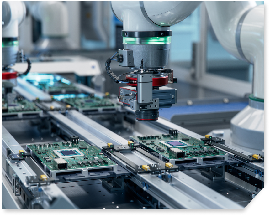
Seamless Assembly for High-Precision
Semiconductor & Photonic Packaging
Our cutting-edge assembly expertise ensures precise chip-to-package integration with industry-leading sub-micron active alignment, high-density interconnects, and heterogeneous integration. We specialize in complex optical and electronic assemblies for AI accelerators, 5G networks, and next-gen computing, delivering high-reliability solutions that optimize performance and reduce time to market.
LEARN MORE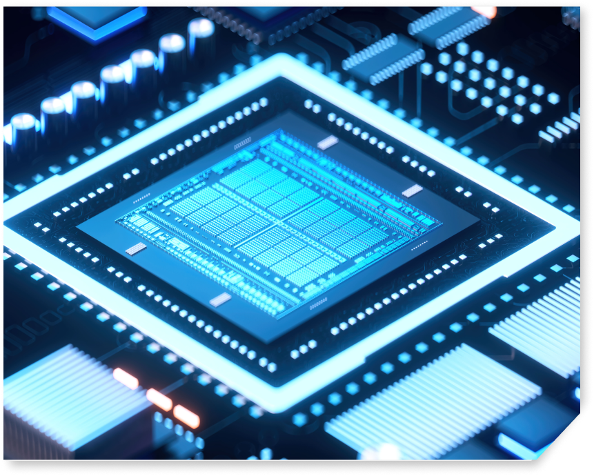
Breakthrough Chiplet Integration for
Scalable, Next-Gen Systems
Silitronics empowers the future of electronics with advanced chiplet integration—merging diverse dies on precision-engineered interposers for optimal signal, power, and thermal performance. Our expertise in modular floor planning and heterogeneous assembly accelerates high-bandwidth, low-latency connectivity that’s essential for AI, HPC, and 5G. From concept design to rigorous validation, Silitronics helps customers bring complex systems to market—faster, smarter, and more reliably.
LEARN MOREOur Services Spectrum
Precision-Driven Design for
Next-Gen Semiconductor
& Photonic
Packaging
From concept to layout, our advanced design expertise ensures seamless integration of chips, substrates, and interconnects. We optimize signal integrity, power efficiency, and thermal performance to meet the demands of AI accelerators, quantum computing, and high-speed photonic systems. With deep engineering insights, we design scalable, high-reliability solutions for the future.
LEARN MOREFabrication for AdvancedSemiconductor & Photonic Packaging
Our state-of-the-art fabrication facility delivers high-precision multi-layer substrates tailored for AI, HPC, and Silicon Photonics. With expertise in organic and ceramic substrates, fine-pitch interconnects, and high-density integration, we ensure superior reliability, scalability, and manufacturing excellence. From prototypes to high-volume production, we bring innovation to life with precision.
LEARN MOREHigh-Precision Wafer Dicing
We deliver advanced wafer dicing using precision blade and laser technologies to ensure clean die separation with minimal chipping. Optimized for high yield and low particle contamination, our dicing supports next-gen semiconductor packaging and performance.
LEARN MOREPowering the Future at the Speed of Light with Photonics
Silicon Photonics is transforming high-speed computing, AI clusters, and next-gen data transfer. Our expertise in sub-micron active alignment, optical integration, and high-bandwidth packaging ensures low-latency, energy-efficient performance. From LiDAR to AI-driven interconnects, we deliver cutting-edge photonics solutions that push the limits of speed, scalability, and efficiency.
LEARN MORESeamless Assembly for High-Precision Semiconductor & Photonic Packaging
Our cutting-edge assembly expertise ensures precise chip-to-package integration with industry-leading sub-micron active alignment, high-density interconnects, and heterogeneous integration. We specialize in complex optical and electronic assemblies for AI accelerators, 5G networks, and next-gen computing, delivering high-reliability solutions that optimize performance and reduce time to market.
LEARN MOREBreakthrough Chiplet Integration for Scalable, Next-Gen Systems
Silitronics empowers the future of electronics with advanced chiplet integration—merging diverse dies on precision-engineered interposers for optimal signal, power, and thermal performance. Our expertise in modular floor planning and heterogeneous assembly accelerates high-bandwidth, low-latency connectivity that’s essential for AI, HPC, and 5G. From concept design to rigorous validation, Silitronics helps customers bring complex systems to market—faster, smarter, and more reliably.
LEARN MORECase Studies
Flawless execution, rapid prototyping, and first-pass success for cutting-edge automotive LiDAR technology.
Flawless execution, rapid prototyping, and first-pass success for cutting-edge automotive LiDAR technology.
Download case studyAccelerating Innovation in 4K Live Streaming & Gaming Cameras
First-pass success, rapid prototyping, and precision execution for breakthrough imaging technology.
Download case studyHigh-Yield, High-Precision IC Packaging for 5G & RF Innovation
Reliable, flexible, and high-performance IC packaging solutions, ensuring uninterrupted supply and exceptional quality.
Download case studyGet in touch
Interested in our end-to-end advanced semiconductor and photonics (PIC) packaging solutions?
Share your details for an expert connect.